Photonic Device Testing Solution for High-Volume Manufacturing
How multi-site array alignment and integrated metrology can reshape the economics of silicon photonics testing.
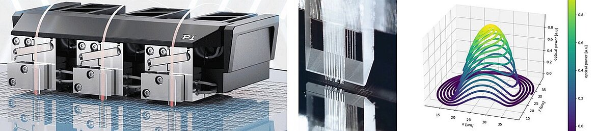
As silicon photonics moves from niche applications into AI infrastructure, hyperscale data centers, co-packaged optics, and next-generation networking equipment, manufacturers face a growing challenge: how to test photonic devices quickly, accurately, and cost-effectively at scale.
As AI infrastructure, hyperscale data centers, and next-generation networking continue to scale, the industry is rapidly approaching the limits of traditional electrical interconnects. Photonics is no longer a niche application; it is becoming a foundational component of modern computing architectures. Yet one critical challenge remains: manufacturing photonic devices at scale without letting test costs dominate the business case.
Energy, Bandwidth and Distance: Where Photonics Is Becoming Essential

While photonic integrated circuits (PICs) promise dramatically lower power consumption and higher bandwidth than traditional electrical interconnects, packaging and testing remain among the largest contributors to overall manufacturing cost. Industry studies have repeatedly shown that test and packaging can represent a significant portion of the total cost of a photonic device, creating a major barrier to large-scale deployment.
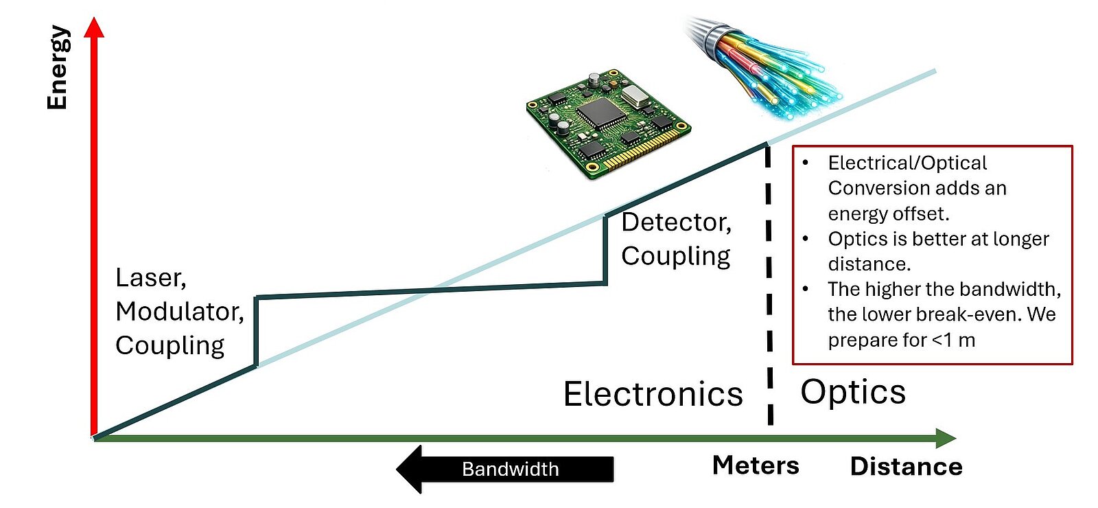
Electrical links still remain efficient over very short distances, but optical communication becomes increasingly advantageous as bandwidth requirements rise. Every electrical-to-optical conversion introduces overhead; beyond a certain combination of distance and data rate, however, optics offers superior energy efficiency and scalability.
This trend accelerates the adoption of silicon photonics, optical interconnects, co-packaged optics (CPO), and advanced photonic integrated circuits (PICs).
Why Photonics Changes the Test Equation
Why Photonics Changes the Test Equation
As data rates continue to increase, electrical interconnects become increasingly inefficient over longer distances. Optical communication offers substantial advantages in bandwidth and energy consumption, particularly as the industry moves toward co-packaged optics and optical connectivity closer to the processor.
However, photonics introduces a challenge that electronics manufacturers rarely face: optical alignment.
Unlike electrical probing, where contact pads can tolerate positional variation, optical coupling often requires sub-micron translational alignment and extremely precise angular positioning. Small variations in fiber position, mode-field diameter, grating coupler geometry, or wafer topography can significantly impact optical performance.
As a result, photonic testing has traditionally relied on serial alignment processes that limit throughput and increase manufacturing cost.
The Hidden Challenge: Test Costs
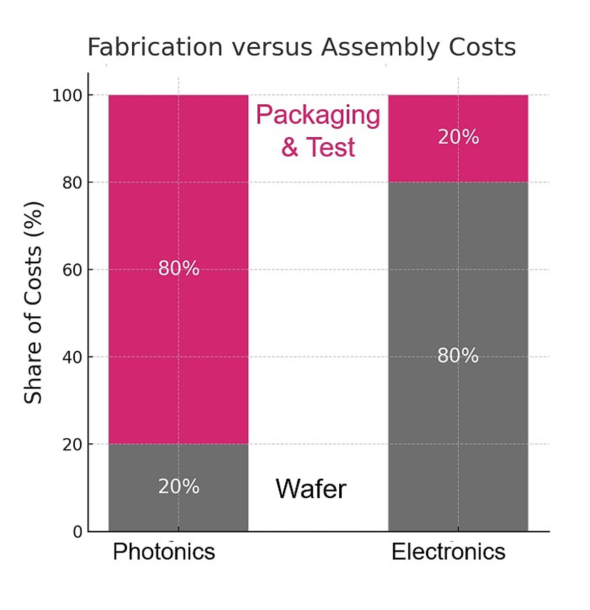
Industry studies consistently identify packaging and testing as the largest contributors to overall photonic device costs. Unlike electronic devices, photonic components require precise optical coupling during testing, creating stringent alignment requirements.
Manufacturers face two major obstacles:
- Throughput Limitations as Optical Tests Are Serialized and Slow. Traditional optical testing is inherently serial. Each optical interface must be aligned individually before meaningful measurements can occur.
- Expensive Design-for-Test Requirements. To compensate for alignment challenges, photonic devices often incorporate additional Design-for-Test (DFT) structures, increasing complexity and cost.
Enabling Scalability: Parallelized Multi-Site Array Alignment in Electro-Optical Wafer Probing
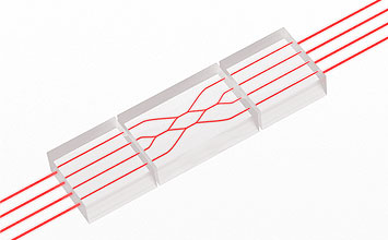
A promising strategy is simultaneous multi-site array alignment, where multiple optical interfaces are aligned concurrently rather than one at a time. By performing parallel optical alignment, test throughput scales with the number of active alignment sites, dramatically reducing overall test time while improving manufacturing efficiency.
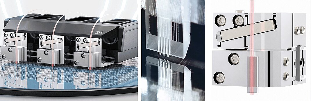
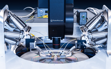
To enable this capability, miniaturized nanopositioning systems could be integrated directly into probe cards (the same platforms widely used today for electrical wafer testing). This approach transforms conventional electrical probe cards into advanced electro-optical test platforms, allowing optical alignment and electrical characterization to be performed simultaneously based on the specific architecture of each photonic integrated circuit (PIC).
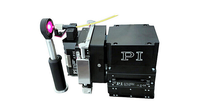
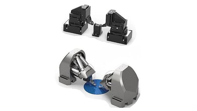
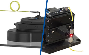
To support this vision, PI has developed an ultra-compact generation of piezo-driven alignment engines specifically designed for dense, parallel integration. In the first prototype phase, each alignment engine occupies a volume of approximately 20x20x20 mm³, making it small enough to be integrated directly into wafer probe cards without significantly impacting their mechanical footprint.
As a proof of concept, three independent PI piezo alignment engines were successfully integrated into a prototype system capable of performing simultaneous optical alignments on separate fiber arrays across a 4-inch silicon photonics wafer provided by LioniX. This demonstration validates the feasibility of highly parallel optical wafer testing and represents an important step toward scalable, production-ready photonic test solutions.
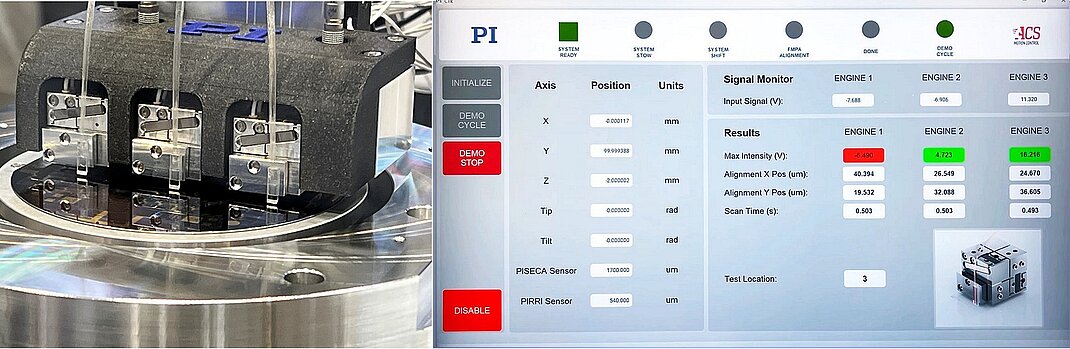
Optimized Alignment in Under 100 Milliseconds
To evaluate system performance, each alignment test was performed using a loopback circuit connecting channels 0 and 4 of a single-mode fiber array. During every alignment cycle, the photonic alignment engine executed high-speed optical scans across a 30µm×30µm search area, rapidly identifying the optimal coupling position.
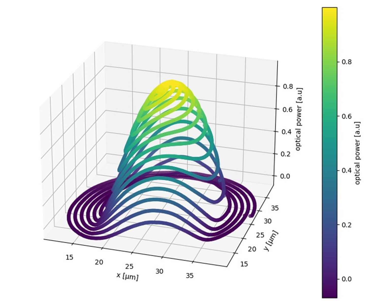
Throughout both factory validation testing and the live demonstration at SPIE Photonics West, the system consistently achieved optimized optical power coupling in less than 100 milliseconds per alignment. This level of speed and repeatability highlights the capability of the alignment engine to support high-throughput, production-scale photonic manufacturing while maintaining exceptional coupling performance.
Moving Beyond Alignment: Integrated Fly-Height Metrology
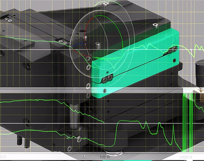
To address one of the industry's most pressing challenges, that is Design-For-Test (DfT); the joint development teams at PI and Keystone Photonics developed an innovative solution by integrating an absolute optical distance sensor, based on interferometric measurement principles, directly into the Fiber Array Unit (FAU).
Unlike conventional approaches that rely on external sensing or design-specific reference features, this integrated metrology solution continuously provides high-precision, absolute distance measurements throughout the alignment and testing process. The sensor enables advanced capabilities including trench detection, surface topography monitoring, and automated height control, providing real-time feedback to the motion system with minimal impact on the hardware footprint.
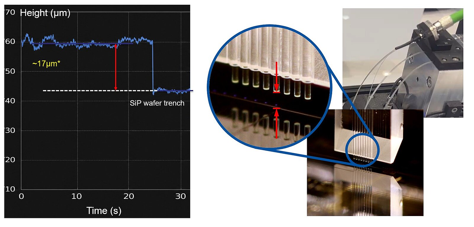
The result is a more robust and automated testing process with improved alignment reliability, greater protection of sensitive photonic devices, and enhanced operational safety. Most importantly, because the measurement is independent of the specific Photonic Integrated Circuit (PIC) design, the solution offers a scalable and versatile platform that can be deployed across a wide range of photonic devices and manufacturing workflows.
By embedding precision optical metrology directly into the FAU, PI and Keystone Photonics are helping simplify test automation while enabling higher throughput, improved process consistency, and greater manufacturing scalability for next-generation photonic devices.
Business Impact of the Parallel Electro-Optics Alignment Solution
- Reduced cost of test
- Increased manufacturing scalability
- Faster time-to-volume production
- Improved return on capital equipment investment
The future of computing increasingly depends on photonics. As co-packaged optics, optical interconnects, and photonic integrated circuits become mainstream, the industry's success will depend not only on device performance and energy cost but also on manufacturing economics.
By combining parallel multi-site alignment, integrated metrology, and closed-loop automation, photonic manufacturers can move closer to a production model capable of supporting the explosive growth of AI, cloud infrastructure, and next-generation networking.


Blog Categories
- Aero-Space
- Air Bearing Stages, Components, Systems
- Astronomy
- Automation, Nano-Automation
- Beamline Instrumentation
- Bio-Medical
- Hexapods
- Imaging & Microscopy
- Laser Machining, Processing
- Linear Actuators
- Linear Motor, Positioning System
- Metrology
- Microscopy
- Motorized Precision Positioners
- Multi-Axis Motion
- NanoAutomation
- Nanopositioning
- Photonics
- Piezo Actuators, Motors
- Piezo Mechanics
- Piezo Transducers / Sensors
- Precision Machining
- Semicon
- Software Tools
- UHV Positioning Stage
- Voice Coil Linear Actuator
- X-Ray Spectroscopy