Advances in Fiber Alignment / Photonics Alignment Automation
History and Future of Active Automated Alignment
From Electronics to Photonics
The first computer link using optical fibers was commissioned four decades ago to safeguard communications from electromagnetic interference at the Cheyenne Mountain strategic command center [1]. Since then we have seen broad adoption of photonic communications technologies in an unfolding pattern of consistently diminishing physical scale:
- As a replacement for costly and laggy satellite links for transoceanic telecommunications
- As the backbone of transcontinental communications, first for voice land-lines and later for data communications
- As the foundation for regional and metropolitan communications infrastructure
- As a delivery mechanism for bandwidth to businesses and consumers, including to the home
- Most recently, as a scalable and high-capacity mechanism for data links across and between data centers, then from rack to rack, then box to box and card to card and soon from chip to chip. IBM has even spoken of a gaudily multi core future chip architecture with hundreds of cores all interlinked by an on-chip optical mesh [2].

This unrelenting drumbeat of advancement and the monotonic diminishment of scale were interrupted by the fiber-optics industry die-back in the early 2000s as overcapacity and an economically unsustainable glut of under-differentiated ventures combined to harrow the field [3]. In hindsight, this bow to “photonomics” seemed inevitable [4] as supply and demand found themselves catastrophically imbalanced. It meant for a quiet decade-and-a-half, but only from a commercial sense. Technologically, the steady down-drop in scale continued in research and industrial laboratories. The goal: elimination of copper as the default interconnect. The promise: bounties of capacity, throughput, parallelism, scalability, and energy savings.
Fiber Alignment Automation Emerges
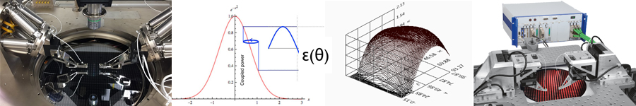
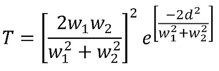
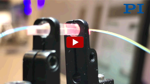
There was a time when testing and packaging a photonic device just meant attaching a single optical fiber to a single emitter or detector. Even in the early days of single-mode fiber optics in the late ‘80s and early ‘90s, this posed significant challenges. Such couplings are typified by a Gaussian cross-section (though departures from the idealized mathematical profile are common). For transverse misalignments of two parallel circular optical waveguides of waist radii and this equates to a transmission that diminishes with lateral misalignment as Equation 1 [5]:
About five years ago, the semiconductor industry began driving photonics, the fruit of advancements in technologies that facilitated the leveraging of light within silicon structures. This merger of technologies reflected a merger of destinies. In the photonics doldrums of 2002, no one was talking about streaming media, Big Data, or the Internet of Things. There were no iPhones with their media-enabled browsers in anyone’s pocket, no GPS apps with always-updated maps, traffic and routing data, no smart factory equipment driving artificially-intelligent prognostics to maximize uptime. Video calls were a fanciful attraction for dazzled suburbanites to gaze upon in AT&T’s Tomorrowland attraction. Music was bought on CDs at record stores, and movies were rented on tape cassettes at Blockbuster. As new wonders swept these aside and became everyday fixtures of civilized life over the past decade (one decade!) as waves of creative destruction washed away entire industries, bandwidth demand proceeded methodically along its exponentiating path. Eventually, the photonics industry came back— because it had to.
As can be readily calculated, in the common case where a misalignment of half a waist radius results in a diminishment of coupling throughput by 1dB; misalignment of a full radius diminishes coupling by a whopping 4dB. The steepening slope of the Gaussian means that drift and other misalignment processes start bad and get worse. It also means that recovering from an initial misalignment is a tweaky process since orders of magnitude of coupling change can result from only a small change in mutual alignment. Multi mode fibers and devices are not necessarily easier to align, since determining the location of their globally optimum orientation is both less obvious and more device- and situation-dependent.
Consequently, the painstaking task of aligning fiber to device was a time-consuming and costly chore beset by poor yields and the necessity for a fine touch. In the late 1980s came the first alignment automation engines, notably the Nanotrak from England’s Photon Control and the FX-1000 from Newport Corporation in the U.S., both of which aligned single-mode fibers to devices, and the Launchmaster from the UK’s York, which automated free-space coupling into a fiber or other device. These mechanisms and their controls not only reduced the fiddly chore of transverse alignment to a few seconds, they could actively optimize the coupling to maintain optimum throughput to address the effects of drifts and disturbances.
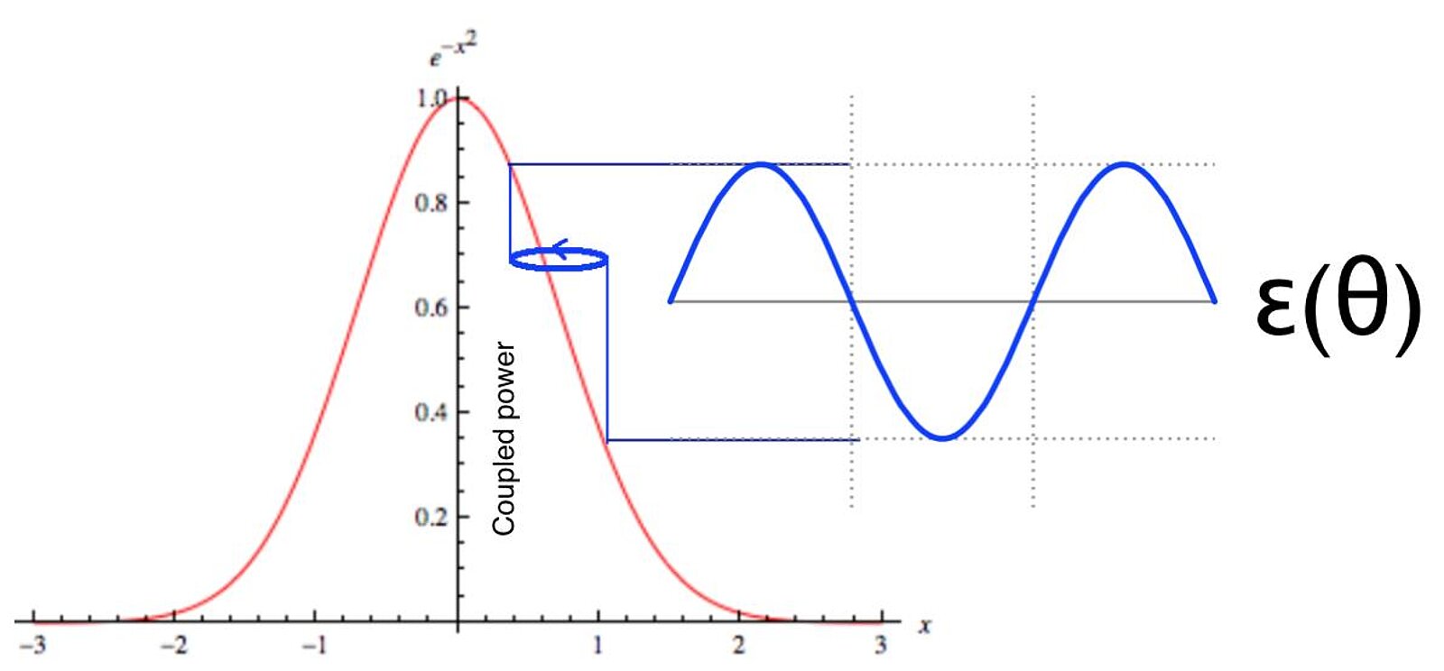
These largely analog instruments employed a simple gradient ascent technique based on dithering one coupled element in a small circle with respect to the other. A detector interposed in the optical path observed the resulting cyclic variation of the coupled intensity. A phase demodulator circuit derived the phase angle between the dither and the varying intensity signal; this indicated the direction along the gradient of the coupling cross-section towards optimum. Meanwhile, the amplitude of the intensity modulation represented the local magnitude of the gradient, providing a measure of lateral misalignment and falling to zero as maximum was reached. Between the direction (phase) and magnitude information, a servo slaved to the optical coupling could be implemented to quickly optimize and maintain the mutual orientation of the devices. This gradient-search technique could align the elements to even the sub-micron exactness required of the then-new single-mode fibers, and keep them aligned in the face of thermal drift and other disturbances.
These gradient-search mechanisms tended to be fragile, offer limited translation and capture range, and/or operate in open loop without position feedback, making them less than optimal for production purposes. These drawbacks began to be addressed with the digital gradient search technology that originated in Newport’s AutoAlign system, subsequently acquired and further developed by ficonTEC. The first digital implementation of a gradient search, it was based on robust, industrial-class precision motion hardware capable of travels of many millimeters. It was quickly implemented into a host of packaging system designs suitable for 24/7 production applications. Its operating principle, documented in US Patent No. 5,278,934 [[6]], involved a point-wise dither followed by a gradient calculation and a resulting corrective motion. The gradient was estimated by observing and among the set of acquired dither points, then calculating an estimate of the gradient as (for example) Equation 2:
A corrective motion was then performed, in the direction of the observed gradient, the step size perhaps proportional to the error signal and subject to limits to prevent overshoot. The process is then repeated. As (the condition of alignment) the system naturally stops when alignment is optimized, yet it can realign when necessary due to drift or other disturbances.
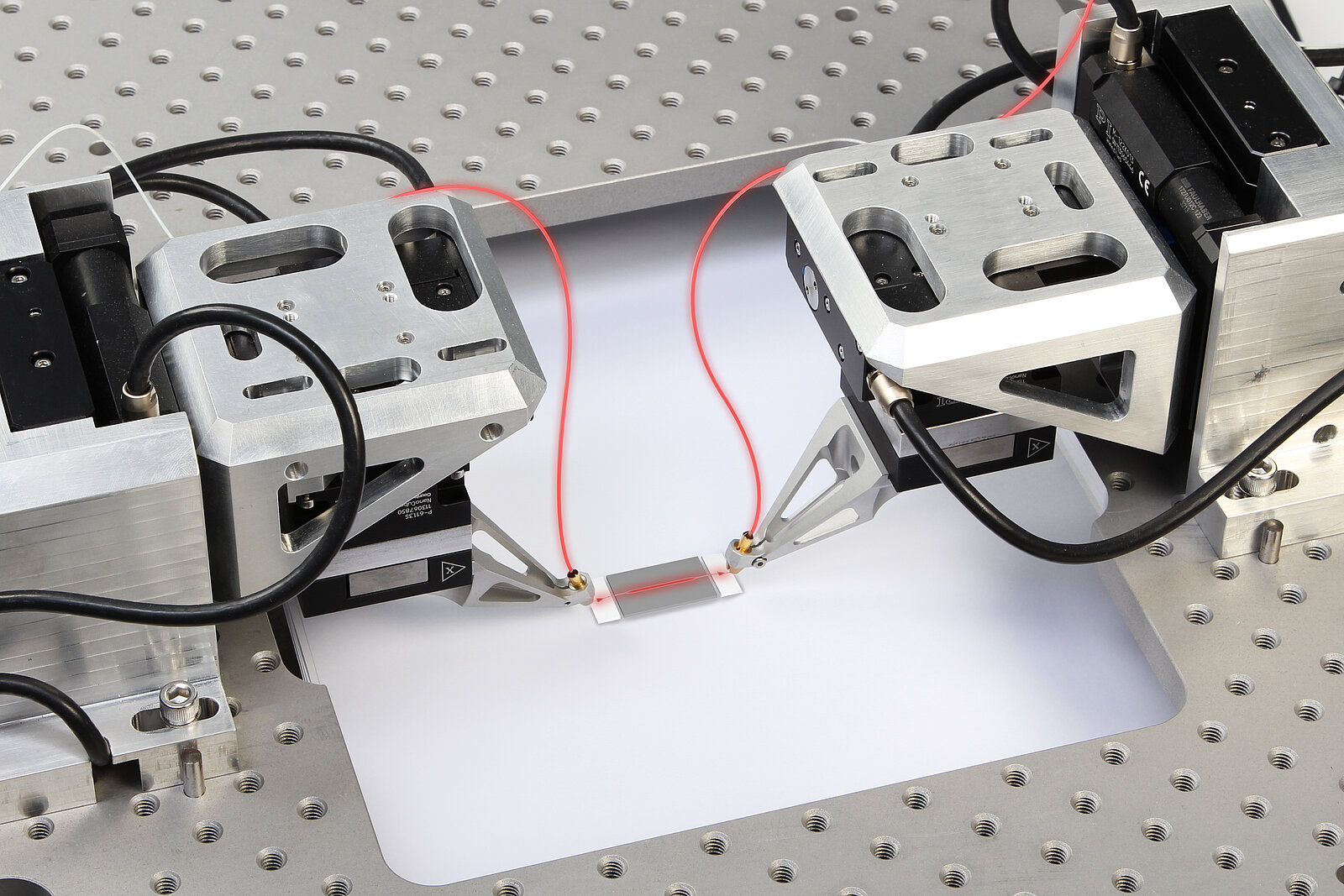
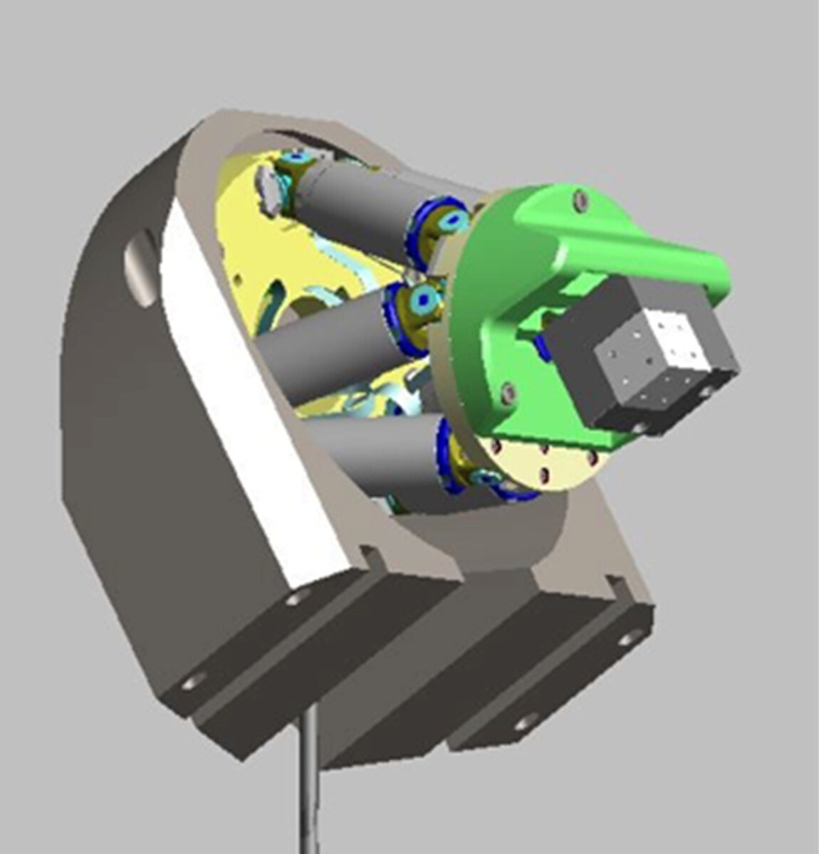
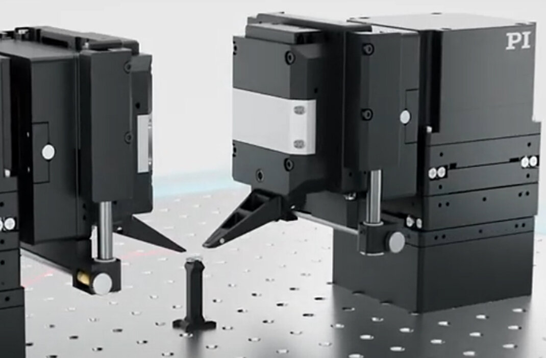
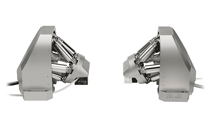
PI’s LightLine alignment system implemented a novel piezo stepping mechanism to achieve similar aims, and in 1997 PI introduced its H-206 photonics alignment hexapod, a micro-robot that implemented its own hill-climbing algorithms and scans and could perform alignments and precision closed-loop motions in six degrees of freedom, with rotations cast by software to any desired center point, such as a beam waist or focal point. This proved essential for the packaging applications that emerged in the industry’s first great blossoming from 1997-2001. Many packaging applications of that era involved angle-sensitive devices, such as confocal optical trains, small lensed assemblies that required alignment in multiple degrees of freedom.
These options served the market well through its original boom phase and then through its long doldrums. But with the advent of Silicon Photonics (SiP), new challenges necessitated new solutions.
SiP Devices Are Different
Silicon Photonics is the fabrication of planar optical devices and circuits, often alongside microelectronics, using materials and processes familiar from integrated circuit microlithography. The dozen years of industry doldrums that began in 2002 allowed the patient development of enabling materials, such as germanium-on-silicon and high-index-contrast films and the requisite building-blocks like couplers, resonators, interferometers, detectors, and the all-important laser integration approaches.
As with microelectronics, SiP devices are formed in layered fashion on the surface of a silicon substrate. The resulting waveguide channels are typically rectangular in format, presenting substantially different optical physics than the cylindrically symmetric geometries familiar from single-mode fibers and most free-space laser applications. Device characteristic dimensions can also be much smaller than was typical back in the halcyon days of photonics’ youth. Often, diffractive couplers are used to kick light out of the wafer plane, making in-wafer devices accessible without dicing and facilitating some packaging approaches for the final devices [7]. Coupling profiles are often asymmetric, astigmatic, and (especially in the case of short waveguide devices) multi mode. It’s common to see coupling cross-sections that have a narrow, knife-edge profile in one dimension and a much broader profile in the orthogonal dimension. And the inputs and outputs of short waveguide devices can interact, with slight changes of alignment position at each of the N inputs potentially steering the aligned position at the M outputs. So for these devices, overall alignment is a moving target on top of it all.
These all add up to significant alignment-process challenges for traditional techniques and mechanisms. The small dimensions and odd, non-circularly-symmetric profiles are problematic for legacy alignment mechanisms and algorithms. And even the simplest waveguide device presents an input and an output, both of which need to be aligned to source and receiving elements such as a laser or fiber. Since input and output can steer each other in many such situations, conventional alignment mechanisms often need to be actuated in an iterative, looping sequence until a consensus alignment is achieved. Add the angular optimization required of arrayed devices and many others, and the alignment process times quickly escalate in an economically prohibitive way. Then there are drift processes, which necessitate similarly complicated and time-consuming sequential realignments.
Puzzles for Packaging …and an Entirely New Consideration
All this poses complication for packaging processes of these devices. Then there’s the fact that the most compelling reason to pursue silicon photonics is of course the ability to stamp out hundreds or thousands of devices in one go on a single wafer. Just as this has enabled the entire digital revolution, so a similar promise is anticipated for exponentiating the adoption of photonics devices.
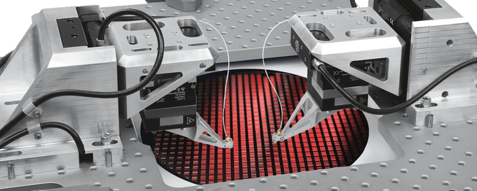
Late in the game, a dawning realization emerged that this meant wafer-level test of photonic elements would of course be required, just as it is for microprocessors and other microelectronic elements. As costly as a fully-patterned wafer is (and their value can exceed several million dollars), it represents a small fraction of its fully-packaged devices’ value [8]. Consequently it is imperative that only known-good devices be allowed to proceed to the packaging phase. Hence, wafer-level testing is needed to identify and exclude faulty devices.
Such testing is performed in the electronic domain as a matter of routine course. Even non-photonic high-value chips tend to be 100% tested at the wafer level, both for bad-part rejection and for grading/binning. An entire ecosystem of wafer-probing tools exists to support this in both lab and fab testing. Conventionally, wafers are cycled into these tools and contacted by an array of electronic probes; lateral probe placement tolerances can be as tight as 20-30μm in today’s designs. Testing then proceeds using a variety of input and output stimuli and signals, often at varying temperatures. In this way, each die is qualified and graded so that its status is known long before dicing occurs.
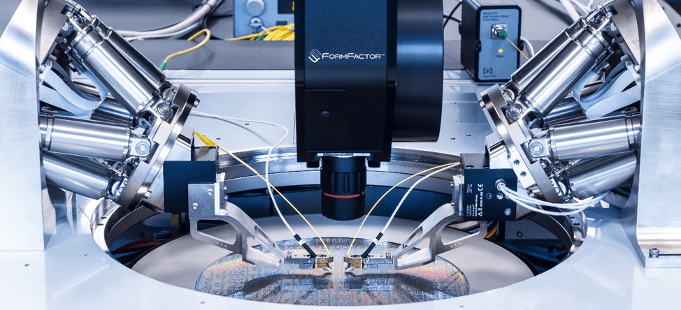
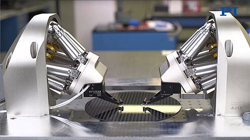
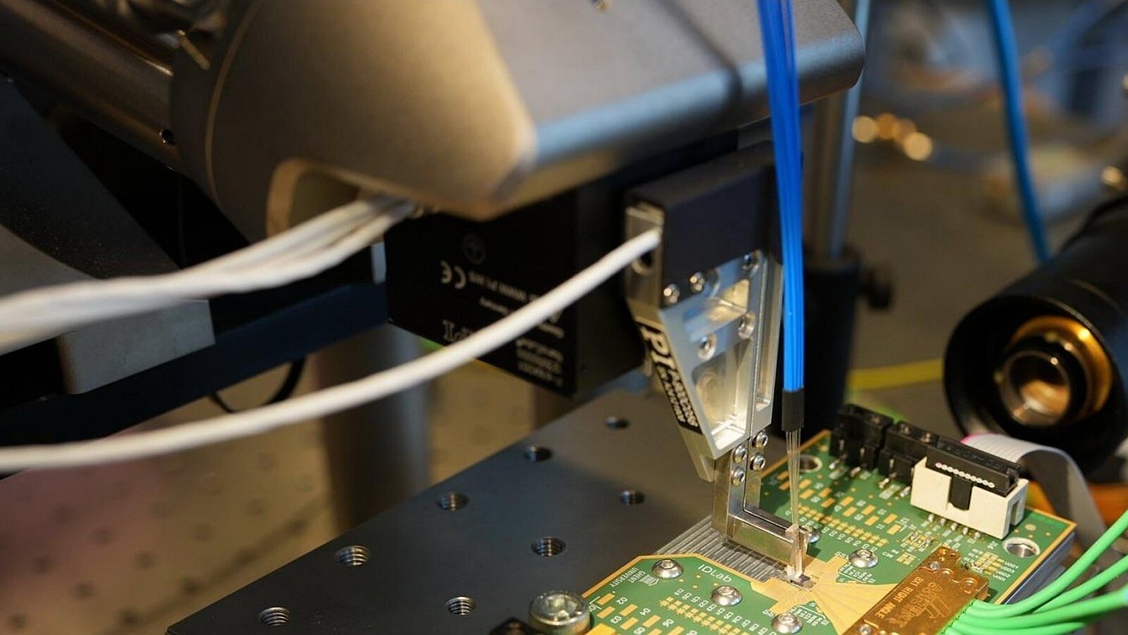
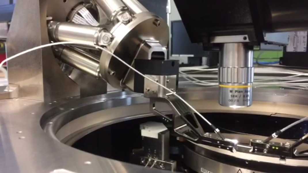
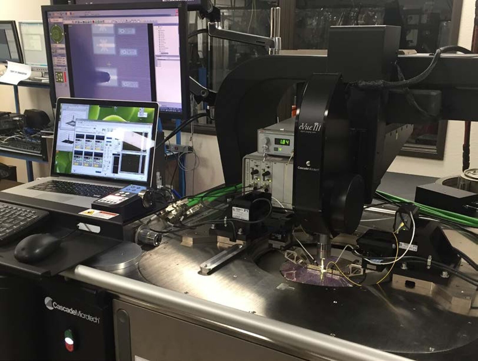
Optical probing presents fresh complications. Contact is forbidden to prevent damage to the wafer and probe fibers or coupling optics. Positioning tolerances for photonic probing are typically two orders of magnitude tighter than for electrical probing, necessitating specialized photonic alignment and positioning mechanisms similar to those traditionally employed in packaging. This in turn places extreme demands on prober structural rigidity and stability and the sub-micron behavior of its positioning stages.
Whereas the packaging challenges posed by silicon photonics represent extensions of photonics-industry practices and processes stretching back 15 or more years, the need for wafer-level test is entirely new. All the considerations already mentioned apply, particularly the economic conundrum posed by the iterative requirement of legacy photonic alignment techniques and equipment when confronted with short waveguide devices, and especially those posing the NxMmultiple input-output alignment issue. These challenges are magnified by the sheer number of devices present on a single wafer.
And bluntly speaking, the cost represented by a fully-patterned wafer eliminates the use of open-loop motion devices, or it should. Only closed-loop devices with real-time position encoding and soft-limit (exclusion zone) capability should be allowed to operate within microns of a costly patterned wafer. To do otherwise is the sheerest false economy, as one broken wafer exceeds the cost of many alignment subsystems. And if the positions of the devices being aligned is not known in real-time to sub-micron precisions, a broken wafer is just a matter of time, and its lost value will represent a large multiple of the saved equipment cost. In addition, incorporation of precision position encoders ensures that when automated alignment concludes, positions are maintained to nanometer-scale stabilities. By comparison, open-loop alignment systems tend to be quite drifty when not actively aligning.

Solve the NxM Problem, Enable the Industry
The economic impasse posed by the testing requirement over the mushrooming number of devices minted on every SiP wafer was recently broken. First, the foundational point-wise gradient search was supplanted in the mid-2000s by a mathematically similar but nonstop approach: PI’s CyberTrack, another all-digital gradient search. This technique, documented in US Patent No. 7,236,680 [9], utilizes a continuous looping dither combined with synchronous observation of position and coupled power, enabling on-the-fly optimization at much higher speeds than the original, discrete approach.
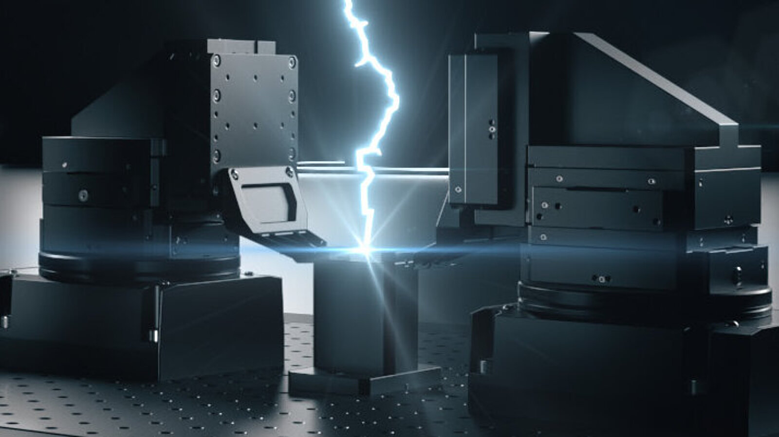
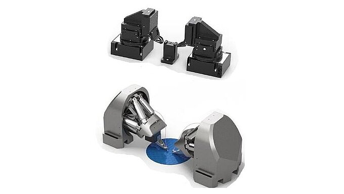
This continuous, all-digital optimization has yielded the newest alignment solution, PI’s Fast Multichannel Photonics Alignment (FMPA) system [10]. As its name implies, this advancement provides alignment of multiple inputs and outputs, and it does so all at once, as it is a technology with inherent parallelism. In the case of short waveguides with their interacting inputs and outputs, it achieves a global consensus optimization in one step, rather than requiring a time-consuming iterative loop. For waisted (most typically, lensed) couplings, optimization of the Z degree-of-freedom can also be performed simultaneously with the transverse alignments, since the Z axis’ power-versus-position curve has a unimodal hill-shape reminiscent of a slice through the Gaussian familiar from transverse coupling profiles. Similarly, angular alignments can be optimized simultaneously, which of course requires mechanics capable of multiple degrees of freedom such as a hexapod, which allows free placement of the rotational centerpoint at or near the beam waist or other optically-desirable location, thereby minimizing parasitic errors. Continuous optimization to accommodate drift and disturbances is similarly active on all inputs and outputs and across all degrees of freedom simultaneously. (The technique is also applicable to fast, parallel multi-DOF alignment of elements in compound lenses.) The technology is of course capable of fast, parallel alignment of multiple, unrelated couplings.
Implementing for Speed
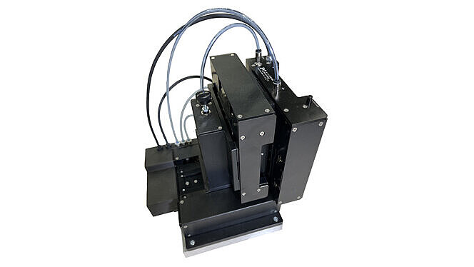
This breakthrough capability is built into the firmware of the alignment controller, providing a significant multiplier of execution speed versus software-driven approaches. The controller drives one or more three-axis piezo flexure stage and three-axis motor stage (coarse positioning/long travel) stacks.
Alternatively, angular optimizations can be achieved by substituting a compact hexapod, with its controller, for a motorized stage stack and controls.
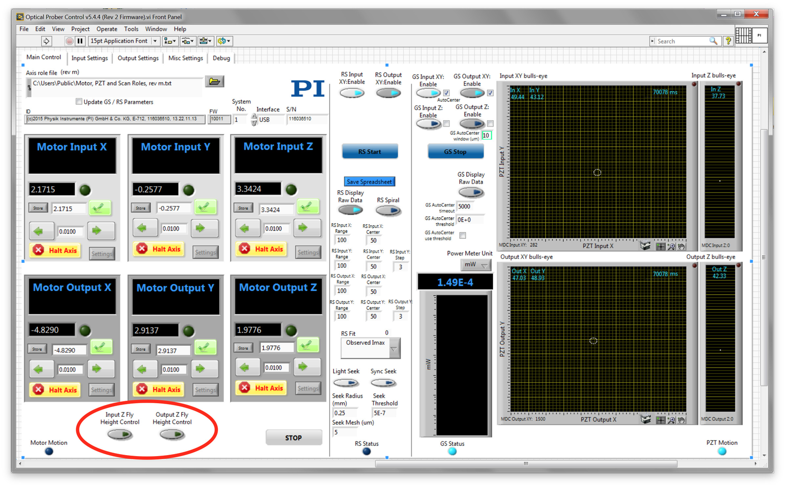
Execution of the firmware-based alignment commands is straightforward and fast. One defines the alignment or scan process by specifying its operational parameters:
- which axes are involved,
- which optical input channel is to be optimized,
- what outer bounds might be desired for an areal scan,
- what dither radius to use for a gradient search, and so on.
Once defined, the user simply issues the “go” command: Fast Routine Start, FRS. This is a very terse command optimized for speed. For a multichannel or multi-degree-of-freedom alignment, several alignment processes can be started together by issuing the FRS command to them all in one command. They will then proceed synchronously to completion.
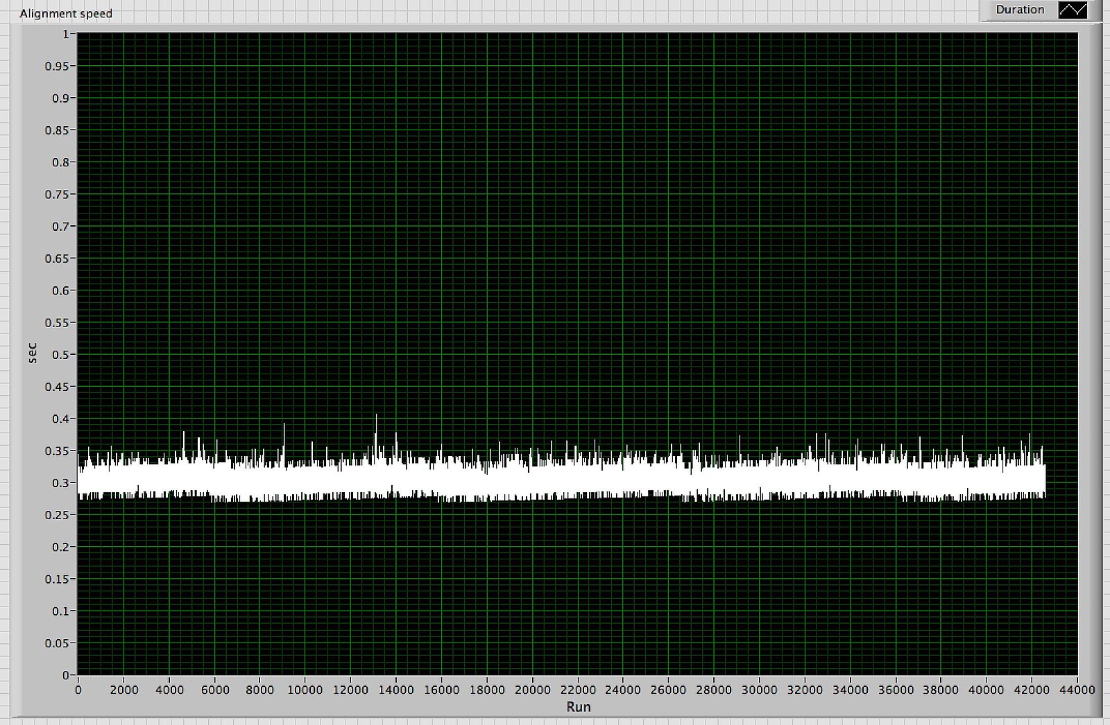
When deployed with the latest nanopositioning hardware, typical gradient search optimizations of SiP devices complete in about 250 – 400msec. In NxM applications, the global alignment time scales slowly with N and M. All told, input/output waveguide alignment is about two orders of magnitude faster than legacy techniques applied sequentially. Even a simple single-coupling alignment is about an order of magnitude faster than was possible with previous techniques.
For alignments that depend on each other (for example, the Z and transverse alignments of a lensed alignment, where the mechanical Z might not be parallel to the optical Z), the user can specify a coupling between any processes, so that (again for example) the transverse alignment does not complete until the Z process completes, preventing the fiber from walking off the beam and ensuring a consensus, global alignment.
Of course, rather than completing when a satisfaction criterion is reached, any process or processes can be told to continue indefinitely, maintaining the global alignment in the face of drift and other disturbances. This is essential for devices incorporating active electronic elements, such as lasers or heaters. Processes may also be instantaneously stopped or re-started at any time. When halted, the dithered device is instantly positioned at the dither center, where it remains, under stable closed-loop position control.
Fast Profiling for Characterization and First-Light Seek
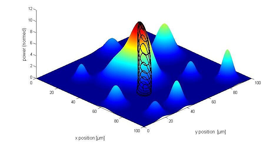
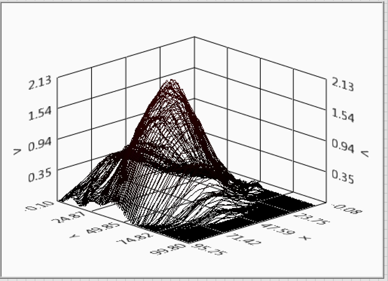
The system also implements fast areal scans using patterns configured for minimal vibration: a sinusoidal raster and a spiral. These take advantage of the wide, 100×100μm travel range of the closed-loop piezo nanopositioners generally used with these systems. That travel range represents a 25X larger capture area than is typical of entry-level, open-loop nanopositioners often deployed in lab-class alignment applications. The sinusoidal raster is similar to a conventional serpentine scan, only without the vibration-inducing two-axis stop/start at the beginning and end of each scan-line. Since it is a single-frequency motion, structural resonances are not driven, leading to significant improvements of execution speed through elimination of settling intervals. This technique is also kinder to applications where small optical devices are held in tweezers, since the high accelerations inherent in each scan-line’s move-and-settle are eliminated, resulting in much gentler actuation despite the high speed of the process. Typical full-field scans are complete within 200 – 400msec.
The spiral scan is similar: again, single-frequency and suitable for sensitive mechanical-optical setups. Its circular scan pattern is more ideal for situations of limited clearance, such as fiber-through-a-hole package designs. Typical scan times are similar to those of the sinusoidal raster.
The controller implements an internal data recorder capable of synchronous, simultaneous acquisition of multi-axis position and optical power at up to 10 ksamples/sec. This is useful for metrology of devices and couplings, which can be an important process metric. Once acquired, the bloc of data can be retrieved from the controller at high speeds via its USB or multiconnection-capable TCP/IP Ethernet ports in parallel with other process execution.
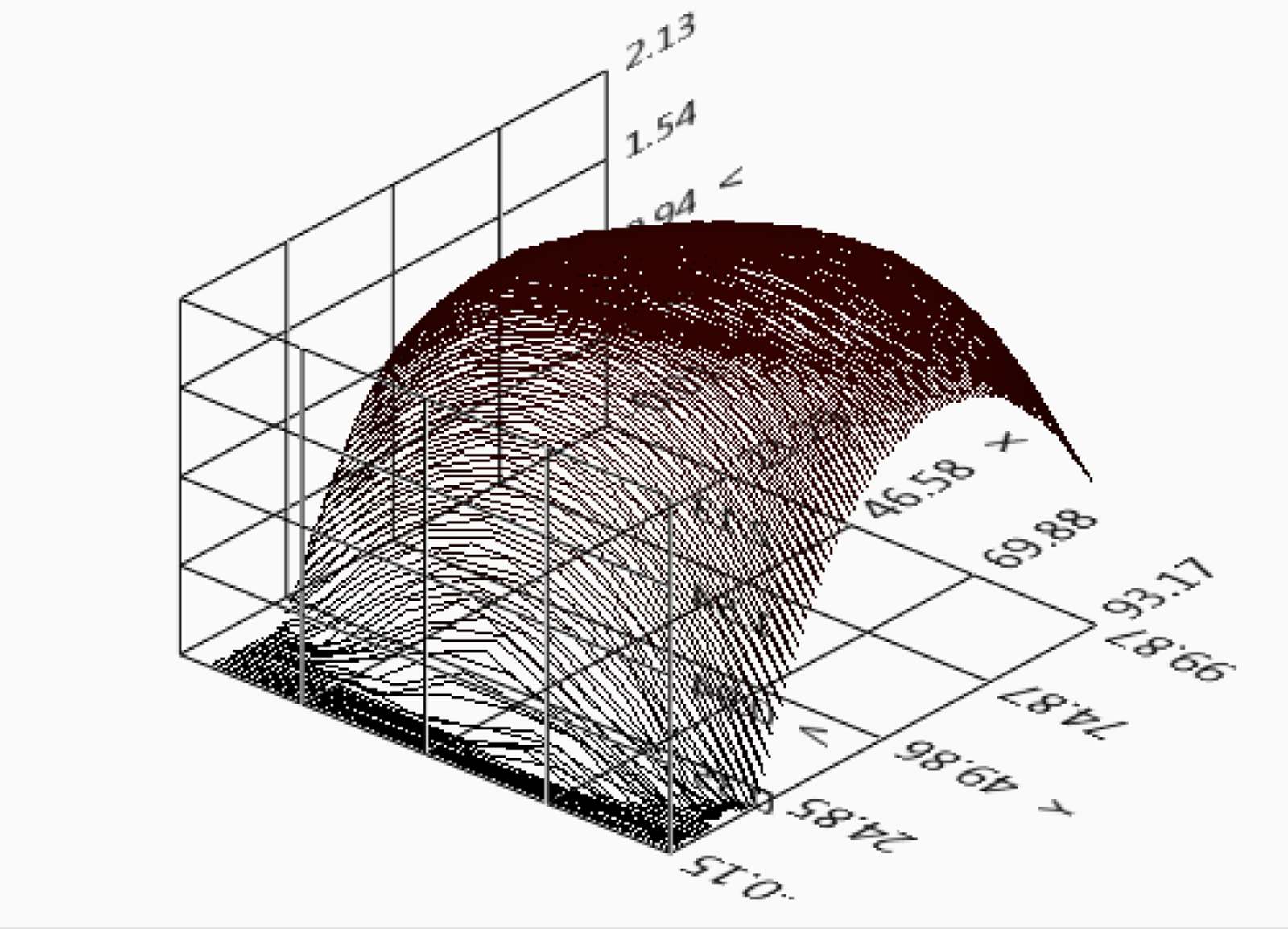
The areal scans are supplemented by the controller’s internal modeling capability that can accurately calculate the position of maximum coupling using only a sparse (that is, fast) data acquisition. This means dense scans are not needed, further speeding execution; the modeling calculations themselves complete in under 1 msec. Modeling is also provided for flat-topped (“top-hat”) couplings, such as encountered when a comparatively large-area deposited photodetector is probed by an optical fiber of respectively smaller core dimension. It is also seen in Differential Mode Delay measurements when a small-core-diameter fiber is scanned across a large-core-diameter fiber. Such a flat-topped coupling profile cannot be aligned using a gradient search since there is no unique point of optimum coupling (or if there is one, it might be due to a tilted optical Z axis and lies on the edge of the flat top, an unstable position). But the areal scan combined with the modeling (which adds sub-millisecond execution time) will localize the true centroid of such a coupling very quickly. This is the position of most robust coupling for such devices.
Often the best strategy is a hybrid one: perform an areal scan to localize the approximate position of each coupling’s optimum, then command the gradient search to optimize all the couplings in order to achieve the global optimum in one step. Depending on fixturing accuracies and device-to-device consistency, the initial localization step can sometimes be omitted after the first device is aligned.
Solving the First-Light Detection Problem
In 2024, a revolutionary method of solving the first-light detection problem was introduced at the SPIE Photonics West conference. The new technique is based on highly responsive mechanics and a controller with integrated AI-based real-time executive function. The fully automated and virtually instantaneous process eliminates the need for extensive calibration or manual intervention. With high frequency data sampling replacing fine pitch scanning, alignment speeds are raised significantly.
Once first light is detected, the FMPA fast gradient search algorithm takes over, utilizing real-time feedback control to swiftly optimize the alignment in parallel across the degrees-of-freedom and channels. Depending on the application, a tracking algorithm can be activated to maintain maximum coupling efficiency. Tets have shown improvements of more than two orders of magnitude in dual-sided alignment and one order of magnitude in single-sided alignment applications. The larger the search area and the more complex the alignment, the more significant the gain. The new, PILightning-dubbed first-light search method is immediately available on PI’s air bearing-based F-143 multi-axis photonics alignment system as well as ACS-based NanoCube and steering mirror controllers.
Conclusion: An Architecture that will Endure… and Enable
FMPA represents a clear break from the past, in ways that are highly relevant to the advent of Silicon Photonics. Previously, alignments were generally sequential and slow. With FMPA, they are parallel and fast. Areal scans optimized for speed and compatibility with today’s tiny micro-optical elements are also built into the system firmware, enabling automated alignment of devices that formerly required a laborious, software-driven approach. Up to six degrees of freedom of optimization are supported per coupling. Fast, fab-class interfaces speed communications to computers, with network-compatibility for integration into production information systems.
Multiple connections are also accepted, so a fab dashboard can monitor the activities of multiple systems simultaneously with control by one or more local or remote computers. For rapid application development and supportability, a rich mnemonic command set provides deep functionality for alignment and precision motion and is supported by dynamic libraries (.dll for Windows, .dylib for MacOS, .so for Linux) and applications libraries for LabVIEW, MATLAB, Python and other popular architectures. A powerful graphical user interface example, constructed in LabVIEW and locally or remotely scriptable by Python, MATLAB and other environments, is offered.
Introduced in 2015, FMPA is available to engineers, researchers and OEMs and is already built into packaging and probing tools from some of the most respected integrators in the industry.
PI has direct sales and applications support offices in key markets around the world. Contact your local office for more information or email info@pi-usa.us.
Author: Scott Jordan, Sr. Director, NanoAutomation® Technologies, Head of Photonics, PI (Physik Instrumente) L.P., scottj@pi-usa.us
Footnotes:
[1] “Handbook of Research on Telecommunications Planning and Management for Business” IGI Global.
[2] “IBM Researchers Develop World’s Tiniest Nanophotonic Switch to route optical data between cores in future computer chips.” Accessed October 30, 2016. www-03.ibm.com/press/us/en/pressrelease/23700.wss
[3] Jordan, Scott. “Photonomics: Automation Approaches Yield Economic Aikido for Photonics Device Manufacture,” 4771:49–60, 2002. doi:10.1117/12.482175.
[4] Jordan, Scott. “The Coming Economic Crunch in Photonics… and What You Can Do About it” 2001, Information Gatekeepers, Inc.
[5] Boudreau, R., Boudreau, S. “Passive Micro-Optical Alignment Methods” 2005, CRC Press.
[6] Jordan, Scott C. “Throughput maximizing systems for substantially unimodal throughput profiles.” 5278934, filed March 18, 1991, and issued January 11, 1994. www.freepatentsonline.com/5278934.html.
[7] See, for example, Poon, A. et al, “Integrated Photonics Research in China”, 2011, Optics and Photonics News, www.osa-opn.org/home/articles/volume_22/issue_9/features/integrated_photonics_research_in_china/
and Sohlström, H. et al, “Apodized waveguide-to-fiber surface grating couplers”, KTH Royal Institute in Stockholm, www.kth.se/en/ees/omskolan/organisation/avdelningar/mst/research/optics/apodized-waveguide-to-fiber-surface-grating-couplers-1.315473
[8] Van Parys, Wouter. 2009, University of Ghent. “Optimization of an Integrated Optical Isolator Based on a Semiconductor Amplifier with a Ferromagnetic Metal Contact.”http://hdl.handle.net/1854/LU-4333564
[9] Jordan, Scott C. “Aligning apparatus and method using on-the-fly determination of throughput-profile gradient for current positioning of radiated influence supplier and/or receiver.” 7236680, filed August 16, 2004, and issued June 26, 2007.http://www.freepatentsonline.com/7236680.html
[10] “Fast Optical Alignment for SiP Production.” Accessed October 31, 2016. https://www.pi-usa.us/en/tech-blog/fast-optical-alignment-for-sip-production/


Blog Categories
- Aero-Space
- Air Bearing Stages, Components, Systems
- Astronomy
- Automation, Nano-Automation
- Beamline Instrumentation
- Bio-Medical
- Hexapods
- Imaging & Microscopy
- Laser Machining, Processing
- Linear Actuators
- Linear Motor, Positioning System
- Metrology
- Microscopy
- Motorized Precision Positioners
- Multi-Axis Motion
- Nanopositioning
- Photonics
- Piezo Actuators, Motors
- Piezo Mechanics
- Piezo Transducers / Sensors
- Precision Machining
- Semicon
- Software Tools
- UHV Positioning Stage
- Voice Coil Linear Actuator
- X-Ray Spectroscopy