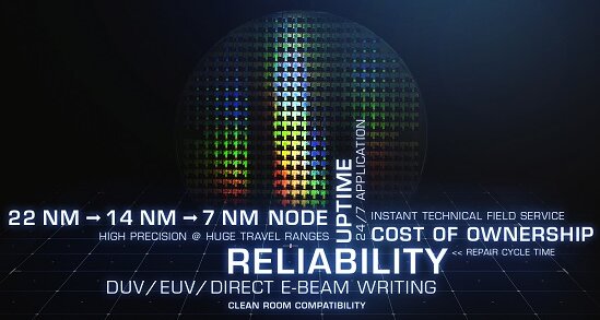
Nanometer precision was not really required when Intel developed their first microchips. The structure widths of the Intel 4004 processor back in 1971 were a generous 10 microns, or 1/100 of a millimeter, humongous compared to today’s structures of 10 nanometers and less. That’s 1,000 times smaller on a 1-dimensional scale, but 1,000,000 times on a planar level. This shrinkage process, known as Moore’s law, stipulates a doubling of the number or electronic circuits every 18 months. This development was predicted by Gordon Moore, co-founder of Intel, back in 1965.
Lately, the integration of photonics and electronics (Silicon Photonics) has led to another step forward both in performance and reduction of power consumption, important when it comes to the environmental impact of the huge server farms required for cloud computing and Big Data applications. Basically, miniaturization of semiconductor components is a combination of faster, cheaper, more economical, and more reliable – higher integration means fewer individual components and thus, lower risk of failure.
Precision Motion, Alignment and Nanopositioning Solutions for Highly Sensitive Manufacturing Processes
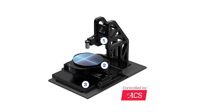
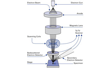
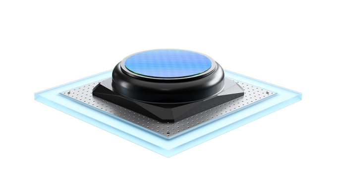
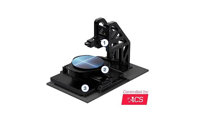
The semiconductor manufacturing and inspection processes are extremely demanding and sensitive. It starts with the pulling of the monocrystalline ingot and continues through to the contacting and final packaging of the finished chip. Advanced nano-lithography is of crucial importance for miniaturization. In the exposure process, which uses state-of-the-art laser sources, the structures for conductor tracks, transistors, and other functional elements are drawn on the raw silicon wafer. When dealing with nanometer sized features, extraordinary precision, tools, and conditions are required: maximum cleanliness, sharp-edged imaging of unimaginably small structures, highly dynamic, coordinated motion of masks and wafers in the lithography machines – the boundaries of what is technically feasible are being pushed ever further from chip generation to chip generation. And PI nanopositioning technology has been instrumental for many years.
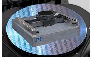
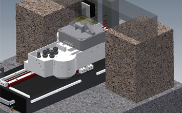
In addition to nano-lithography, PI ultra-high precision motion stages and (sub-)systems are also used in many other process steps in the manufacture of semiconductor components including quality assurance. And PI´s involvement in driving semiconductor progress is literally from the ground up, starting with enabling the most advanced vibration cancellation technologies in sub-floor platforms and tool structures.
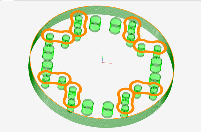
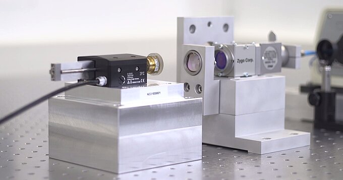
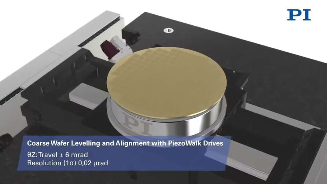
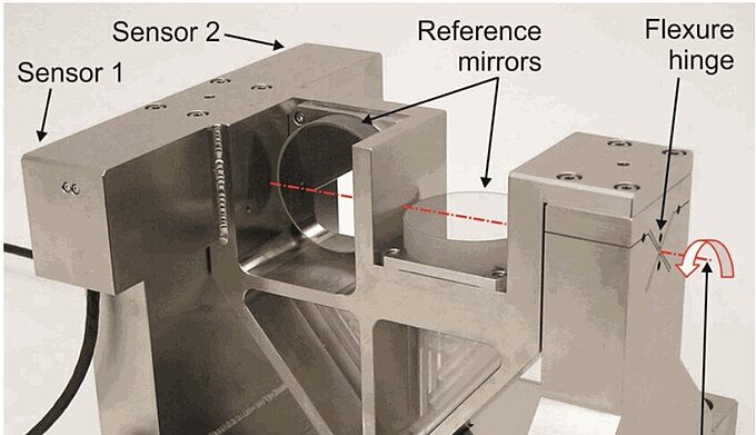
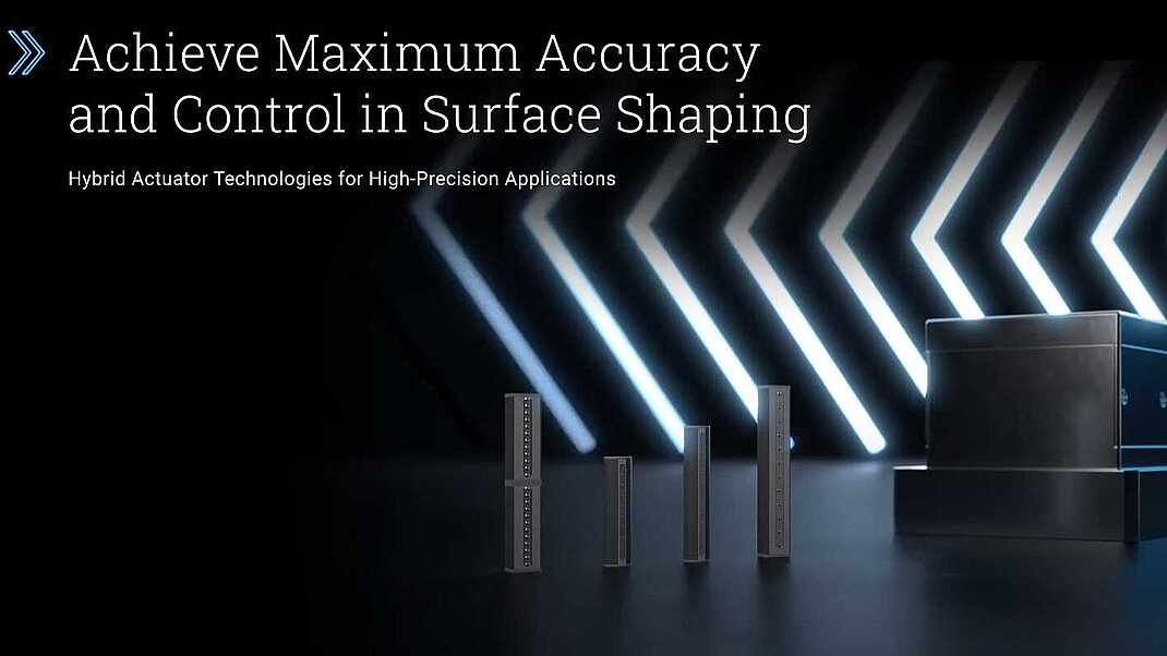
For highly precise beam delivery, laser beam steering tip/tilt systems were developed, combining nanoradian resolution with rapid, millisecond scale response and settling.
A new patented technology allows ceramic shims to be programmed to change dimensions in the nanometer range – a set-and-forget technology that can be used to make minute adjustments to the alignment of optical systems or large mechanical assemblies, correcting for errors that appear after time or with changing temperatures.

The Customer in Focus: Much More than Technology, Components, and Systems
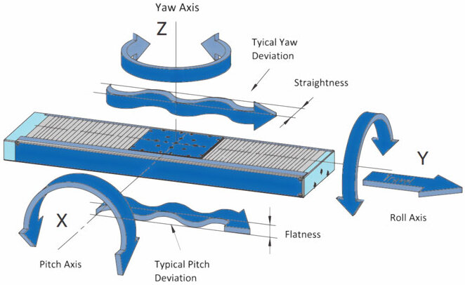
In all of these applications, the ability to precisely control the motion and position of objects with nanometer and even sub-nanometer resolution and high dynamics, or to hold a position precisely over the long term, without power requirements, plays a decisive role.
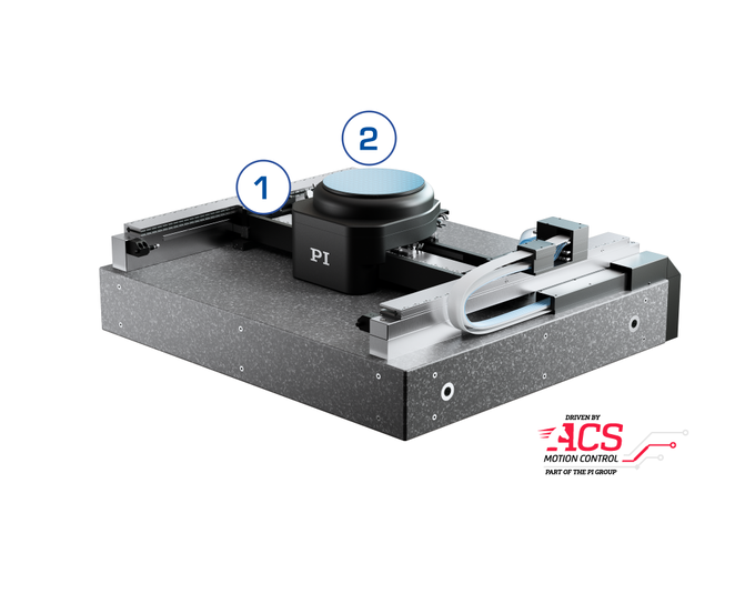
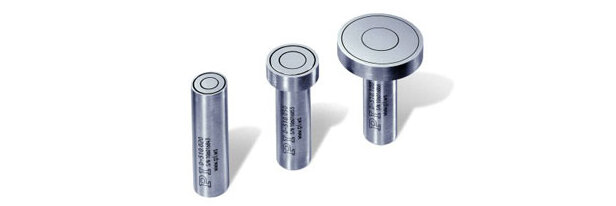
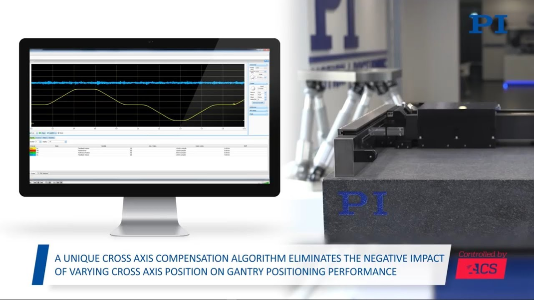
PI offers decades of know-how and a wide range of technologies – including piezo transducers, developed and manufactured in our PI Ceramic subsidiary, sensors, piezo actuators and motors and air bearing motion systems with 3-phase linear motors drives to controllers, software, and firmware – as well as components and systems. Together with our subsidiary ACS Motion Control, a market and technology leader in industrial high performance, EtherCat-based controller technology, we also enable the control of highly complex multi-axis systems for the next generation of demanding applications in semiconductor manufacturing all the way up to EUV-L.
Advanced Design, Copy Exactly, and Global Services
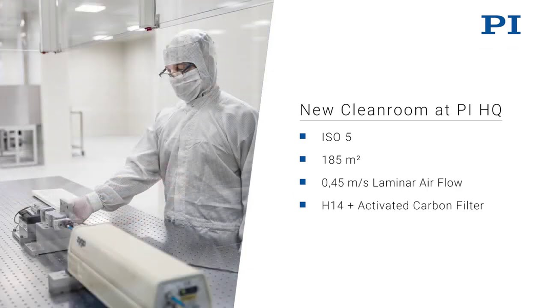
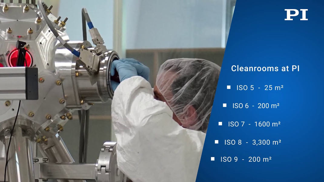
Advanced design alone is not enough. It is our long experience as a supplier to leading system integrators in semiconductor manufacturing that enables us to understand and meet the high demands of this industry. With customer-specific service level agreements (SLA) and a global service team, we can react promptly to disruptions occurring on short notice. To this end, we have set up service hubs with highly qualified staff near the world's most important semiconductor production locations, where we keep spare parts for all critical components and assemblies. Based on extensive long-term tests of our components under a wide variety of climatic conditions and a Copy Exactly strategy, we offer our customers a high level of security against failure from the outset, i.e. high uptime. Also, PI has created clean rooms that even meet the exceptional cleanliness requirements that are required in the manufacture of components for EUV lithography.
On The Way to The Next Big Thing
The success factors of the semiconductor industry, in particular continuous miniaturization of structures, will ensure innovations for a long time to come. And PI has exciting answers ready for the increasing demands on precision in motion control and high-performance positioning. And the semiconductor industry is changing at a faster pace than at any time since the invention of the integrated circuit. While Moore’s Law continues its relentless advance to drive ever-smaller feature sizes and higher performance and efficiencies, it is no longer just about smaller transistors on larger wafers. Now micro-optical components are being fabricated alongside microelectronics, and entirely new computing and communications paradigms are emerging which leverage the mysteries of the quantum world. As the applications change, so do chips, and the revolution proceeds. PI is right there, partnering with the leaders of change.


Brochure: Motion Control and Precision Positioning Systems for Electronics & Semiconductor Manufacturing / Test
High Precision Motion, Automation and Control Solutions for Laser, Semiconductor, and Photonics Applications
Sign up for our Tech Talk: Enabling the Technologies for Semicon