Test, assembly, and packaging of photonics components is a critical step in the manufacturing process. Automation of the alignment process can save cost while increasing throughput. The need for higher performance computing and data-communication speed has led to the advent of silicon photonics. In addition, to higher performance, silicon photonics can also reduce the power requirements of next generation server farms significantly.
Challenges
With the advantages, this new technology also brings about several production challenges, including the need for test platforms for testing of wafers / components prior to wafer dicing, analogous to conventional electrical-test wafer probing, but in the optical domain. Similarly, downstream packaging processes are more exacting and complex than ever.
Read IBM article “Silicon Integrated Nanophotonics Technology: from the Lab to the Fab”.
Multiple Alignments Quickly
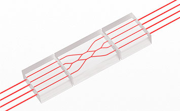
Since many classes of components have one or more inputs plus one or more outputs, and each of these needs to be aligned to nanoscale accuracies in order for test or packaging processes to proceed, it quickly becomes uneconomical to use traditional alignment techniques in a sequential fashion. Plus, the multiple couplings often interact, especially in the case of short waveguides. So a global, parallel, simultaneous alignment-optimization solution is needed.
6DOF Alignment Systems for Silicon Photonics Test and Assembly
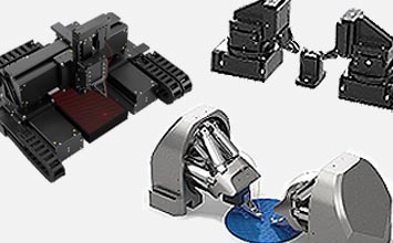
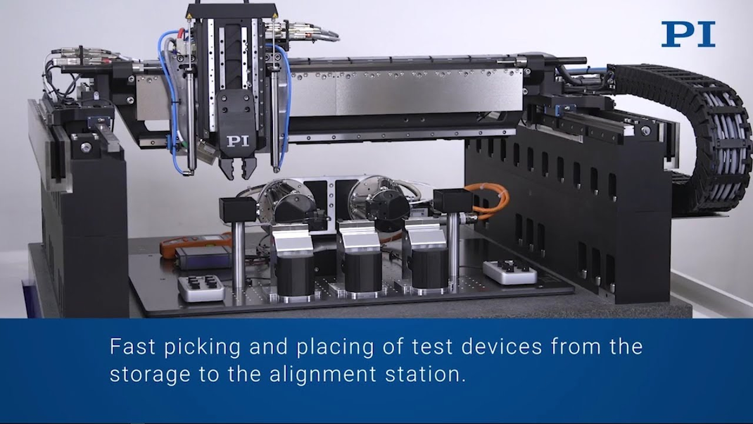
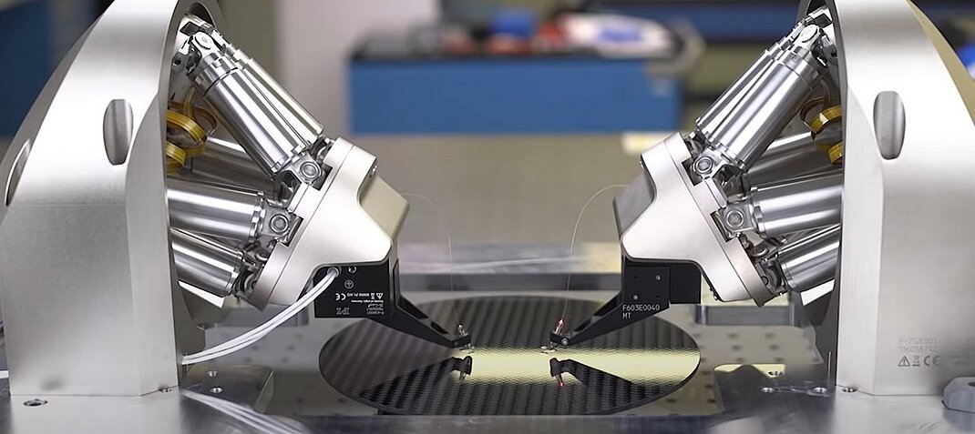
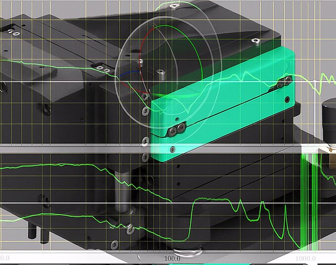
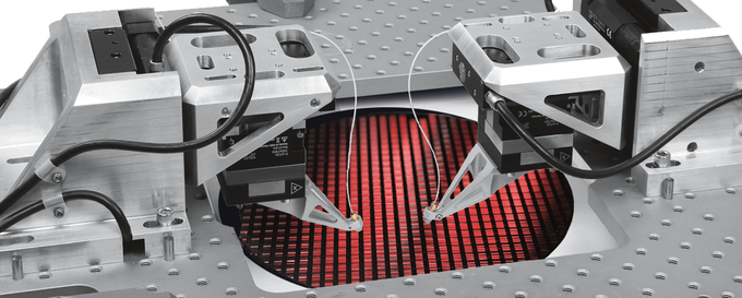
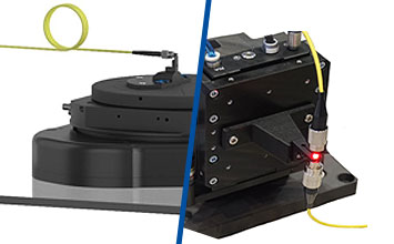
An available solution is based on with PI’s E-712 photonics alignment controller and F-131 Fast Fiber Alignment Stage, a hybrid approach, where a coarse position is approached with a compact motorized positioning device (50 nanometer resolution) integrated with a high-speed piezo nanopositioning mechanism.
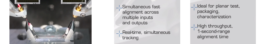
The video below demonstrates the capabilities. In this demo, an in-wafer, grating-coupled waveguide device is simulated by a short length of single-mode fiber. Its input and output are coupled via lensed fibers mounted on grippers on PI’s 6-Axis-Hexapod / XYZ piezo scanner combination, controlled by the E-712 controller.
Features and Benefits of the Alignment System
- Fast, fab-worthy alignment from wafer to package
- Nanoscale alignment accuracy
- Sub-second typical scan and alignment times
- Any number of channels and degrees of freedom
- Built-in scan and align algorithms
- No external compute resources
- Automatic alignment of upright and tilted SM, MM & top-hat couplings
- Integrated data recorder
- LANTCP/IP-compatible interface
- Simultaneous fast alignment across multiple inputs & outputs
- Real-time, simultaneous tracking
- Ideal for planar test, packaging, characterization…
- Comprehensive software resources: host software, drivers for most programming languages, sample code, intelligent tools
- Platform-independent design
- High-level ASCII command set
- Easy implementation


Blog Categories
- Aero-Space
- Air Bearing Stages, Components, Systems
- Astronomy
- Automation, Nano-Automation
- Beamline Instrumentation
- Bio-Medical
- Hexapods
- Imaging & Microscopy
- Laser Machining, Processing
- Linear Actuators
- Linear Motor, Positioning System
- Metrology
- Microscopy
- Motorized Precision Positioners
- Multi-Axis Motion
- Nanopositioning
- Photonics
- Piezo Actuators, Motors
- Piezo Mechanics
- Piezo Transducers / Sensors
- Precision Machining
- Semicon
- Software Tools
- UHV Positioning Stage
- Voice Coil Linear Actuator
- X-Ray Spectroscopy