Case Study: Photonic Array Device Assembly
Advanced Motion Control is the Key to Better Productivity

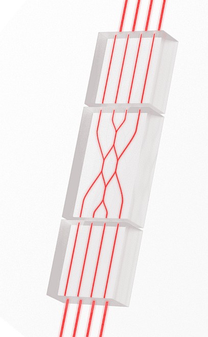
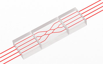
Optical fiber arrays are essential devices for high-speed, large-capacity optical communication and data processing systems. These systems, leveraging optical fibers, have become widely adopted due to their ability to transmit and receive enormous amounts of data efficiently. Aligning optical fiber arrays to integrated photonic circuits (PIC) or waveguides quickly and with minimum signal loss is crucial for meeting the demands of the photonics industry. There are passive and active fiber optical alignment techniques that can be used, the latter one providing better coupling efficiency and much greater flexibility, when the latest break-through alignment algorithms are applied.
PI’s Fast Multichannel Photonic Alignment (FMPA) technology was introduced in 2016. It quickly amassed prestigious honors like the R&D 100 Award and the Lightwave Innovations Award for its revolutionary ability to perform multiple alignment processes in parallel, for example:
- For elements whose positional optimization depends on other elements. Examples include waveguide structures whose inputs, outputs and channels can interact, such as short waveguides whose inputs and outputs “steer” each other. Other examples include lenses or diffractive elements in imaging or resonator assemblies whose mutual positions are interrelated. FMPA can perform these optimizations in one go, yielding a global optimization that is often 100 times faster than previously possible.
- For alignments in multiple degrees of freedom. A ubiquitous example in Silicon Photonics (SiP) is any array device, where alignment motions in ThetaZ (common notation for rotation about the optical axis) cause dealignment in XY. Previously, any corrective motion in ThetaZ necessitated a pause and a realignment in XY, meaning array alignments required a lot of time. FMPA’s parallel alignment capability allows the full device alignment to be performed in one quick step, since the compensation of the geometric errors due to ThetaZ motions occurs in parallel with them.
This rapid reduction of global alignment time has proven to have a profound impact on test and assembly cost for photonic products. It is well established in industry literature that alignment is the largest contributor, overall, to product cost[1]. Since alignment must be performed many times across multiple process steps in the test and assembly of photonics devices, FMPA’s dramatic reduction in process time is highly leveraged.

There are similarities between the Silicon Photonics industry and the young semiconductor industry of the mid-1980s. Today, you can build a fab just by issuing purchase orders, but that was not the case 35 years ago. Consequently, the players of that era--such as IBM, which dominated the semiconductor industry--built their fabs around bespoke tools constructed by systems integrators who were often captive or internal.

The situation is similar in Photonics today. There have not been enough toolmakers to satisfy demand, and there has been little incentive for them to progress beyond legacy automation principles dating to the short-lived Photonics boom of 1997-2002. That boom was driven by one dominant end application: long-haul telecommunications, supplanting satellite-based approaches. That is quite unlike today’s broadly diverse end-application base, which sees exponentiating data consumption spanning needs as diverse as social networks, personal health, Big Data, the Internet of Things, and even selfies. Still, the painful memories of that era linger and have contributed to hesitation by potential new toolmaker entrants. That is finally starting to change with entrants like FormFactor with its groundbreaking Cascade wafer probers and Tegema with its Integrated Photonics Assembly tools, but it has meant that Photonics players and their contract manufacturers have often chosen to design and build their own production tools, just as IBM did in the ‘80s.
What is Fiber Array Alignment?
In optics and photonics, array alignment involves the precise positioning of optical fibers or collimators to couple light with photonic chips (often referred to as photonic integrated circuits or PICs), waveguides or other optical devices. This enables the PICs to utilize light for tasks such as data transmission, sensing, or computation. To minimize losses, it is critical to maximize optical power through all channels of the fiber array, which requires sophisticated alignment hardware and algorithms, especially when time is of the essence in production environments.
Production Example
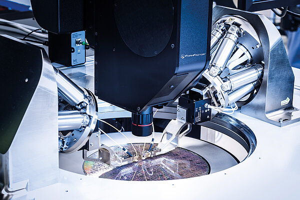
It is necessary to protect the identity of most PI customers, so we will refer to this rather typical user as Substantial Photonic Company, or SPC. SPC manufactures networking hardware. Their devices incorporate photonic chips with multiple I/O channels, along with other elements such as lasers, photodiodes and fiber arrays. After probing[2], the chips are singulated and proceed to packaging.
Attaching the fiber arrays to the chips is one of the fundamental steps in SPC’s packaging process and will be our example here. For the reasons elaborated in the last section, SPC chose to build its own tooling. Not incidentally, this enabled them to leverage the latest alignment technology for this process (and others): PI’s FMPA.
In this and most other SiP alignments, the quantity that must be optimized is the optical power traversing the multiple channels of the device[3]. We tend to see three ways of conveying the signal from devices to PI’s controllers during test and assembly alignment:
- Optical monitor trap. Here a portion of the optical throughput through the device or channel can be directly accessed. Often this is leveraged to perform assorted metrologies on the device during test and assembly, such as spectroscopy. Inclusion of a high-bandwidth optical power meter is straightforward in these circumstances. PI’s FMPA controllers incorporate high-speed analog inputs for this purpose. So, an optical power meter with an analog output is needed. Select meters like PI’s own F-712.PM1 are optimized for fast alignment, providing the necessary fast signal together with a logarithmic response, yielding many benefits including eliminating auto-ranging (which would otherwise need to be disabled) and providing especially extensive capture capability due to the multi-decade dynamic range.
- Photocurrent tap. Here the optical throughput through the device or channel can be measured by an on-device photodiode or similar element. The resulting photocurrent is accessible to the outside world. Connecting this to a high-bandwidth transimpedance amplifier provides the signal that can FMPA’s alignment rapidly optimize. An external photodiode input on the F-712.PM1 meter can provide this easily, together with the benefits of the wide dynamic range from its logarithmic response.
- RSSI port. Some devices’ optical signal can only be measured by interrogating their Received Signal Strength Indicator port, typically via I2C or SPI. In a production alignment workstation, a simple microcontroller (such as an Arduino) is regularly employed to perform these queries rapidly in a loop, converting the numeric response to each query into a voltage to drive the FMPA process.

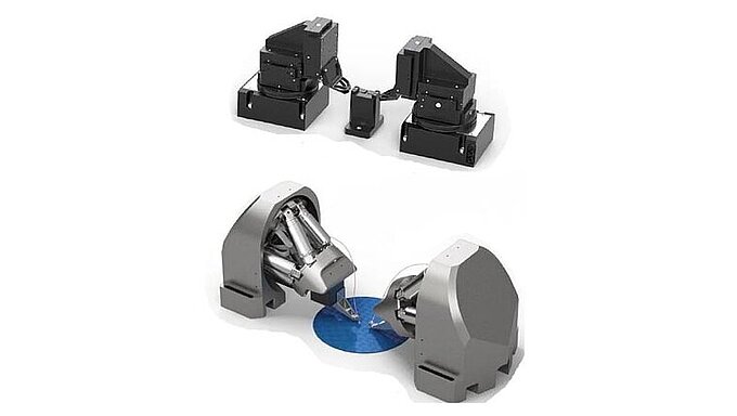
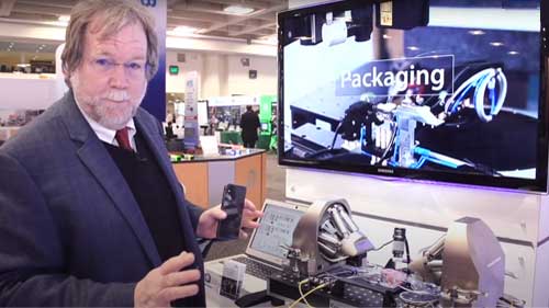
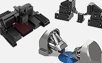
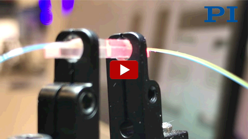
SPC uses a mix of these in their applications. To perform the fiber-array attachment, SPC chose PI’s F-712.HU1 FMPA system (Figure 3), deploying a multitude of these at their contract manufacturer. The alignment of the fiber arrays to the silicon photonic chip proceeds as follows:
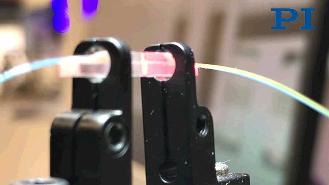
- The fiber array is brought into near proximity to the chip. SPC’s production processes are highly controlled, so their initial Z gap is repeatable to a few microns. Note: Other customers often must set or validate the Z gap. This can be accomplished via several possible methods:
- Vision. The field of machine vision has been broadly democratized in recent years, with the advent of excellent, USB-connectable cameras that can reduce the need for costlier “pro-grade” machine vision cameras and frame grabbers. Powerful and accessible vision frameworks like http://OpenCV.org and intelligent cameras like http://OpenMV.io make quick work of device-presence detection, edge detection, squaring and gap setting.
- Contact. FMPA systems are available with optional force sensors with milligram-level sensitivity. Some customers use these to bring devices into contact, establishing the Z=0 condition. Then the motion system can be commanded to back off to a desired gap.
- Optical geometry. A succession of area scans can be performed at increasing Z, allowing the beam fan-out to be observed and the absolute separation calculated. Since PI FMPA systems incorporate built-in area scan functionality and this is often used for device qualification, this can be a cost-effective approach.
- Waist finding. In some waisted applications such as with a lensed fiber, the FMPA system can perform a gradient search in Z to quickly determine the optimum Z position. An XY gradient search in parallel will keep the alignment on-beam in cases where the mechanical and optical axes are not parallel.
- Proximity sensor. Some device situations can accommodate a proximity sensor such as a capacitive probe, allowing the Z gap to be set directly.
- OTDR. Some device situations can utilize optical time-domain reflectometry to set the gap between two elements.
- In SPC’s application, first light can generally be immediately detected in the first channel of the array thanks to the 6-7 decade dynamic range of the F-712.PM1 power meter. If not, the Nanocube® can find it by performing an area scan over its full 100x100µm range in typically 300msec or less. This is a built-in command in its controller and includes runtime options such as automatic Gaussian fitting. Similarly, the hexapod (which shares nearly identical scan-and-alignment functionality and commands with the Nanocube®) can perform an area scan over ranges from microns to millimeters. The two mechanisms can even scan in parallel, speeding scans to tens of millimeters with scan resolutions down to submicron scales.
- Once first light is detected in the first channel, the Nanocube® can be commanded to optimize lock-onto the coupling with a continuous gradient search. This will fine-align and track the coupling in real time.
- Since the hexapod can rotate about any desired point in space, its pivot point is set near the optical axis of the first channel. The hexapod can then be commanded to perform a ThetaZ optimization on the 2nd channel (The identical approach is used for devices with a U-shaped loop-back channel, as often found for facilitating assembly alignment). Note that the XY lock-on of the first channel automatically accommodates misplacements of the rotational centerpoint, allowing both alignment processes to proceed in parallel— FMPA’s key advantage. Similarly, optimizations of ThetaX/ThetaY can occur at the same time for devices requiring them.
Total time for steps 1-4 is approximately one second. Glue is then applied; the XY tracking corrects any disturbance from this and accommodates drift during the early phases of epoxy polymerization.
System options can include provisions for light-curtain and other safety interlocks, and soft limits are a standard feature for implementing forbidden zones to prevent collisions.
Footnotes
[1] See, for example, “Automated High-Throughput Assembly for Photonic Packaging”, Barwicz et al, Photonics Summit, Cadence, 2017, https://www.cadence.com/content/dam/cadence-www/global/en_US/documents/company/Events/summits/photonics/fortier-2017.pdf and “Process-based cost modeling of photonics manufacture…”, E. Fuchs et al, J. Lightwave Tech., 2006, https://www.semanticscholar.org/paper/Process-based-cost-modeling-of-photonics-the-cost-a-Fuchs-Bruce/125e24b2e2e71860f088526441ee5ce16e6ce42c
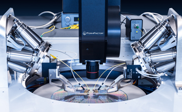
[2] See https://www.youtube.com/watch?v=izM33rfVVc4 for FormFactor’s introduction to photonic wafer probing.
[3] In principle, FMPA can optimize virtually any hill-shaped figure-of-merit that can be measured or calculated with sufficient speed, including things like extinction ratio for polarization-sensitive alignments, calculations of image sharpness for imaging optic assembly, or calculations of beam quality for laser assembly. In addition, PI controllers allow virtually any fast, measured quantity to be used as a servo input, allowing automatic positioning to achieve a desired set-point.


Blog Categories
- Aero-Space
- Air Bearing Stages, Components, Systems
- Astronomy
- Automation, Nano-Automation
- Beamline Instrumentation
- Bio-Medical
- Hexapods
- Imaging & Microscopy
- Laser Machining, Processing
- Linear Actuators
- Linear Motor, Positioning System
- Metrology
- Microscopy
- Motorized Precision Positioners
- Multi-Axis Motion
- Nanopositioning
- Photonics
- Piezo Actuators, Motors
- Piezo Mechanics
- Piezo Transducers / Sensors
- Precision Machining
- Semicon
- Software Tools
- UHV Positioning Stage
- Voice Coil Linear Actuator
- X-Ray Spectroscopy