The new area of silicon photonics is being driven by us. We walk around with supercomputers in our pockets. We consume streaming media. We participate in social networks. We benefit from personalized medicine [on] the Internet of Things.
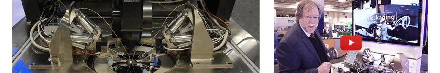
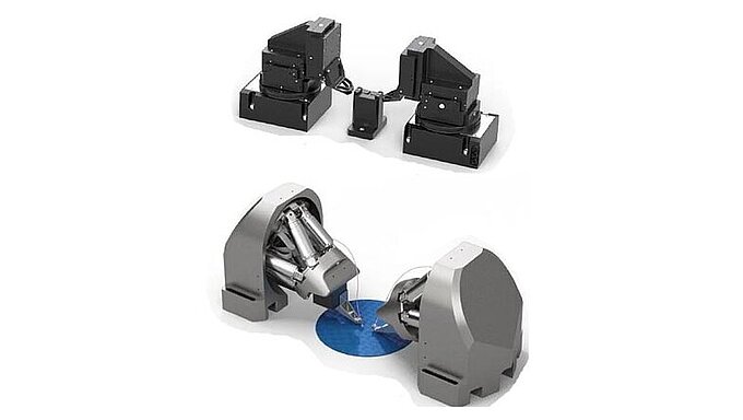
All of these things consume an escalating amount of data, and for reasons of capacity and energy [and] efficiency, the trend has been away from copper interconnects to optical interconnects. Energy efficiency, capacity, [and] scalability [to] distributed architectures for data centers [are] all of these. Our efforts are facilitated by photonic designs. In addition, future plans for new types of computing will definitely involve photonics, so photonic interconnects are increasingly important for all of us and they need to be manufactured. That starts at the wafer-level. This is a wafer prober made by Cascade Microtech, a Division of Form Factor, and it shows how the hexapod micro robots that are manufactured by PI (Physik Instrumente) are used in an embedded application to validate the health of chips prior to the packaging process.
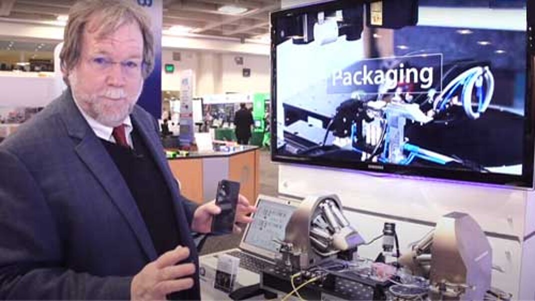
The real costs in making the silicon photonics device is actually in the packaging – you do not want to package a bad device. So the devices are validated and tested at the wafer level using one of these tools. After the chips have been validated on a wafer prober and diced off of the wafer into individual chips, they must be packaged. One of the most important steps for that is to attach fibers or fiber arrays to the chip itself. Our technology is unique in that it can perform input and output alignments and do so in multiple degrees of freedom, all at the same time, in a single step, as opposed to the sequence of steps that used to be required. It's much faster – faster by about a factor of 100.
So here, in this application, you can see the repeating demonstration where we bring input and output fiber arrays to a simulated chip that we have manufactured out of two class arrays connected together. [It’s] simulated, because we can't show our customers’ devices being aligned here. In the first step, the input and output arrays are brought into a rough initial position and then the active alignment is performed to maximize the photonic efficiency of the device of the coupling and then usually our customers will perform some bonding and apparently other operations. The key here is the parallel execution of all of the alignments. It's unique in the world. We can do the multiple degrees of freedom of the multiple inputs and outputs all in one step, so it's significantly faster.
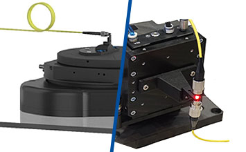
The field is also enjoying a continuing unfolding of new technologies, new devices, and new approaches that are very exciting because they promise continuing growth and continuing innovation in the industry. This is a really good example here - this is a high density interconnect that is pioneered by a company called Chiral Photonics in New Jersey. In this very slender probe, there are up to 91 individual single-mode channels that can be used to connect to a very high density photonic chip. Actually, what we're showing here is the ability to align and automatically track the coupling between these high-density chips and the novel high density probe. For more information about these positioning technologies and their importance for research development and manufacturing of silicon photonics devices, quantum computing devices, and anything of this sort, your best first place for information is to contact your local PI applications engineer. We have offices all over the world and we're deeply embedded in these applications from the research to the manufacturing arenas.


Blog Categories
- Aero-Space
- Air Bearing Stages, Components, Systems
- Astronomy
- Automation, Nano-Automation
- Beamline Instrumentation
- Bio-Medical
- Hexapods
- Imaging & Microscopy
- Laser Machining, Processing
- Linear Actuators
- Linear Motor, Positioning System
- Metrology
- Microscopy
- Motorized Precision Positioners
- Multi-Axis Motion
- Nanopositioning
- Photonics
- Piezo Actuators, Motors
- Piezo Mechanics
- Piezo Transducers / Sensors
- Precision Machining
- Semicon
- Software Tools
- UHV Positioning Stage
- Voice Coil Linear Actuator
- X-Ray Spectroscopy