


Piezo Ceramics Manufacturing Process
PI manufactures its own piezo ceramic materials at the PI Ceramic factory.
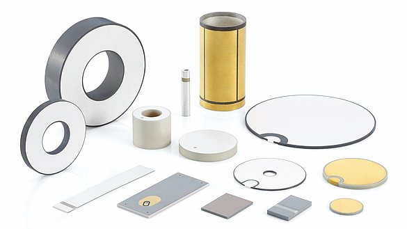
There are two types of ceramics: Bulk ceramics and thin film ceramics.
Bulk Process
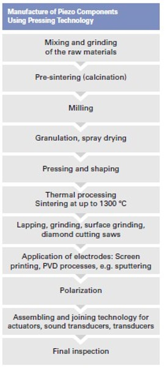
Bulk Process
Piezoceramic bulk elements are manufactured from spray-dried granular material bymechanical hydraulic presses. The compacts are either manufactured true to size, taking into account the sintering contraction, or with machining excesses which are then reworked to achieve the required precision. The bulk process starts with mixing and ball milling of the raw materials. Next, the mixture is heated to 75% of the sintering temperature to accelerate reaction of the components. The polycrystalline, calcinated powder is ball milled again to increase its reactivity. Granulation with the binder is next to improve processing properties. After shaping and pressing the (green) ceramics is heated to 750° to burn out the binder.
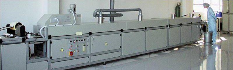
The next phase is sintering at temperatures between 1250° C and 1350° C. The sintered ceramic material is hard and can be sawn cut, ground, polished, lapped, etc., to the desired shape and tolerance if required. Screen printing is used to metallize the piezoelements and sputtering processes (PVD) are employed for thin metallizing layers (electrodes are applied). The sintered elements are then polarized. The last step is the poling process which takes place in a heated oil bath at electrical fields up to several kV/mm.

Thin Film Multilayer Process
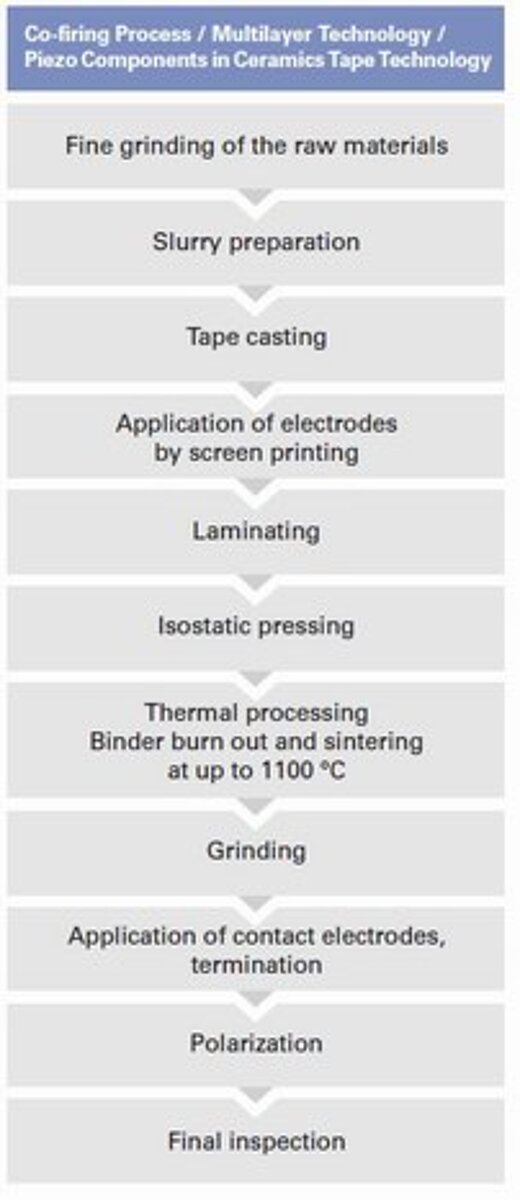
Thin Film Multilayer Process
Multilayer Piezo actuators require a different manufacturing process. After milling a slurry is prepared. A foil casting process allows layer thickness down to 20 µm. Next, the sheets are screen printed and laminated. A compacting process increases density of the "green" ceramics and removes air trapped between the layers. The final steps are the binder burnout, sintering (co-firing) at temperatures below 1100° C, end termination and poling.
All processes, especially the heating and sintering cycles must be controlled to very tight tolerances. The smallest change affects quality and properties of the Piezo material. 100% final testing of the piezo material and components at PI Ceramic guarantees the highest product quality.
Definition of Piezoelectric Coefficients and Directions

Because of the anisotropic nature of Piezo ceramics, effects are dependent on direction. To identify directions the axes, termed 1, 2, and 3, are introduced (analogous to X, Y, Z of the classical right hand orthogonal axial set). The axes 4, 5 and 6 identify rotations (shear).
The direction of polarization (3 axis) is established during the poling process by a strong electrical field applied between two electrodes. For actuator applications the piezo properties along the poling axis are most essential (largest deflection).
It should be clearly understood that the piezoelectric coefficients described here are not independent constants. They vary with temperature, pressure, electric field, form factor, mechanical and electrical boundary conditions etc. The coefficients only describe material properties under small signal conditions. Compound components such as Piezo stack actuators, let alone preloaded actuators or lever amplified systems cannot be described sufficiently by these material parameters. This is why each component or system manufactured by PI is characterized by specific data such as stiffness, load capacity, displacement, resonant frequency, etc., acquired by individual measurements.
Piezoelectric materials are characterized by several coefficients:
Examples are:
- dij: Strain coefficients [m/V]:
strain developed (m/m) per electric field applied (V/m)
or (due to the sensor / actuator properties of Piezo material).
Charge output coefficients [C/N]:
charge density developed (C/m²) per given stress (N/m²). - gij: Voltage coefficients or field output coefficients [Vm/N]:
open circuit electric field developed (V/m) per applied mechanical stress (N/m²)
or (due to the sensor / actuator properties of Piezo material)
strain developed (m/m) per applied charge density (C/m²). - kij: Coupling coefficients [no Dimensionss].
The coefficients are energy ratios describing the conversion from mechanical to electrical energy or vice versa.
k² is the ratio of energy stored (mechanical or electrical) to energy (mechanical or electrical) applied.
Other important parameters are the Young's modulus Y (describing the elastic properties of the material) and the relative dielectric coefficients (permittivity) e (describing the capacitance of the material).
To link electrical and mechanical quantities double subscripts (e.g. dij) are introduced. The first subscript gives the direction of the excitation, the second describes the direction of the system response.
Example:
d33 applies when the electric field is along the polarization axis (direction 3) and the strain (deflection) is along the same axis. d31 applies if the electric field is in the same direction as before, but the strain is in the 1 axis (orthogonal to the polarization axis)
In addition the superscripts "S, T, E, D" are introduced. They describe an electrical or mechanical boundary condition.
Definition:
S = strain = constant (mechanically clamped)
T = stress = constant (not clamped)
E = field = constant (short circuit)
D = electrical displacement = constant (open circuit)
The individual piezoelectric parameters are related by several equations that are not explained here because they are not important for the user of piezo actuators.
If you have any questions, ask a PI engineer for help.