DOWNLOAD DATASHEET
Download Datasheet
MORE INFORMATION
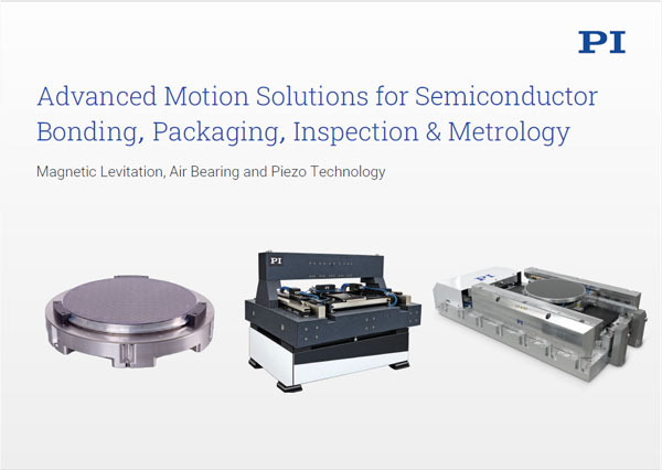
DOWNLOAD | SEMICONDUCTOR BONDING, PACKAGING, INSPECTION & METROLOGY
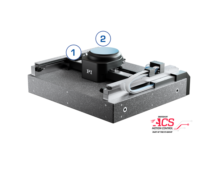
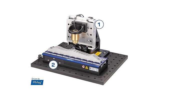
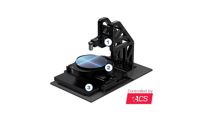
Efficient wafer inspection and metrology are essential for ensuring a stable, high-performance semiconductor manufacturing process. With up to 800 complex production steps, semiconductor fabrication demands precise inspection and metrology at every critical stage to guarantee the highest levels of quality and yield.
Optical inspection is an essential process in industrial quality assurance. Optical inspection systems, which are used in industrial environments, should provide reliable and repeatable measurement results and enable high throughput rates.
The entire chip manufacturing process consists of 400 to 800 production steps. At all critical points in the manufacturing process, inspection processes are essential to ensure the high quality and reliability of the final products.