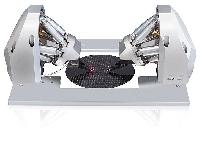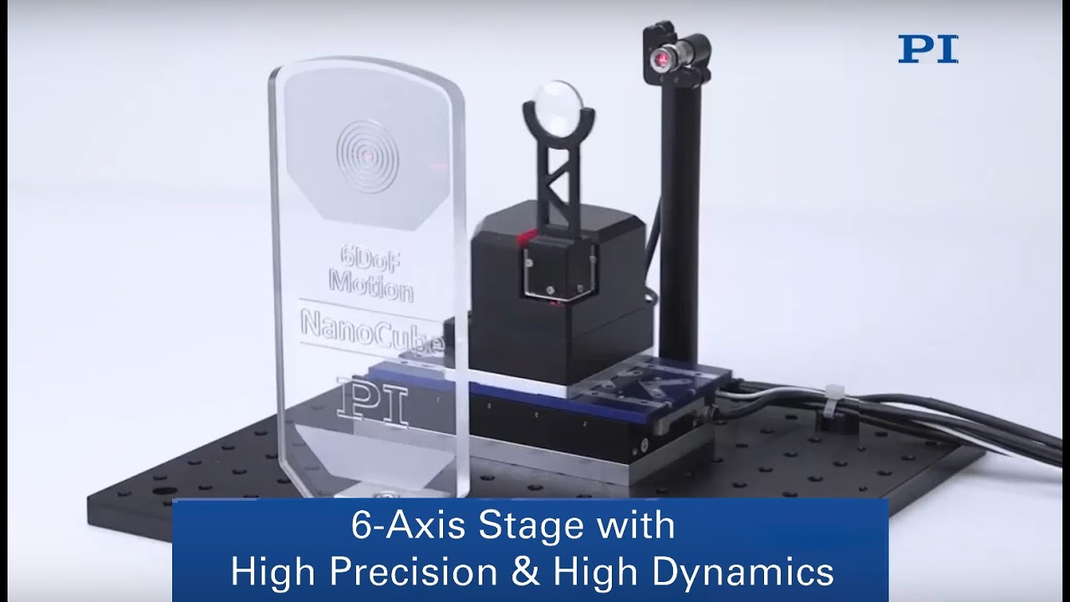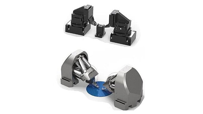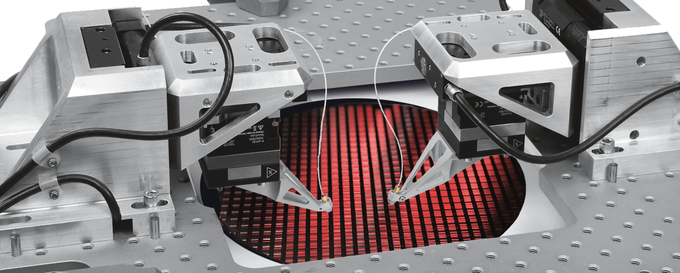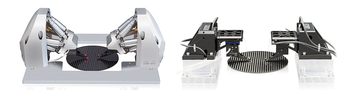
Silicon Photonics (SiP) is essential for meeting the world’s appetite for data. PI’s groundbreaking new industrial technologies are making it happen. In both test and packaging, PI automation subsystems allow SiP fabricators and their tool OEMs to cost-effectively and reliably test and package this new generation of photonics devices with the required nanoscale precisions and high production throughputs. Key to this is PI’s unique capability of automating fast alignment across multiple interacting inputs and outputs and degrees of freedom all-at-once, often achieving global optimization in less than a few hundred msec. This inherent parallelism eliminates the time-consuming iterative approaches formerly required to orient multichannel SiP components for test and packaging, resulting in time savings that can exceed two orders of magnitude. Because different devices and production applications present different requirements, PI’s modular architecture offers solutions for virtually all production test & packaging needs.