Automating Photonics Alignment, Fiber Alignment

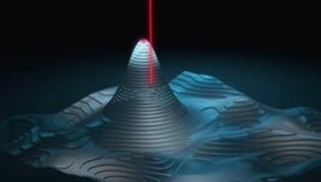
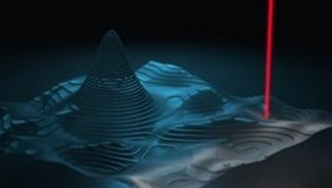
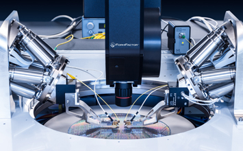
Integrating photonic components, such as waveguides, lasers, photodiodes, and multiplexers, onto a silicon chip introduces numerous testing challenges, not only at the wafer level. From conceptualization to series production, a substantial volume of performance data for each element is essential for successfully conveying the structure's design and ensuring its qualification. Given the significant process costs involved in SiPh chip production through final packaging, early identification of defective chips is imperative. This early detection allows for their removal from the manufacturing process, thereby minimizing potential losses and optimizing the overall efficiency of the production workflow. 

World’s Fastest Alignment Algorithms and Alignment Engines

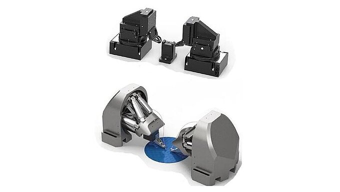
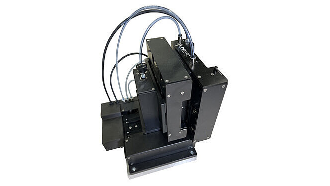
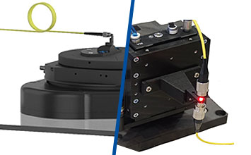
The process of automating the alignment of fibers, waveguides, fiber optic arrays, lasers etc., especially the time it takes for each alignment is a major cost driver in silicon photonics test and packaging. Automated alignment systems with PI’s advanced algorithms and mechanics are the solution to the problem – cutting down on alignment time by orders of magnitude while achieving ultralow-loss alignment performance with arrays with 0.02dB typical coupling repeatability.

Product Overview: Photonics Alignment Automation / Automated Fiber Alignment

Selection of Individual Fiber and Photonics Alignment Products

Background Information and Articles on Photonics Alignment – How does it Work?

PILightning – Solving the First-Light Detection Problem

Active Alignment - Fast Multichannel Photonics Alignment

Active Alignment

The need to align devices down to nanoscale accuracy is arising in many fields. Optical components such as the lenses or lens assemblies in small cameras, or even the CCD chip itself, need to be positioned with ever more precision.

PI Fast Photonics Alignment Solutions Running on ACS Motion Controllers

Photonics Alignment White Paper

Advances in Fiber Alignment / Photonics Alignment Automation

Emerging Resources for Photonic Device Manufacturing

Photonics Array Device Assembly

Case Study: Photonic Array Device Assembly

The Quantum Era Emerges - How PI Fast Automated Alignment Enables Practical Manufacturing

LIDAR - Smart Active Alignment

Active Photonics Alignment Demos

SiPh Wafer Probing

The integration of photonic structures or elements on a silicon chip presents, already at wafer level, a multitude of new challenges for the testing technology of these elements. In order to transmit the design of the structure, from the concept through its qualification up to series production, a very large amount of performance data of the respective element is required.

Physik Instrumente – Photonics Assembly

Assembly & Packaging of Photonic Devices

Modern passive optical networks (PON) rely on optical components that can split or combine light signals coming from high-power light sources. Replacing active components with passive components provides significant cost savings by eliminating the need to power and service active components in the transmission loop.

Why Fast Steering Mirrors are used in Laser Communication / Free Space Optical Communication

Webinars Explaining Photonics and Fiber Optics Alignment

Ubiquitous Photonics, Universal Challenges
Learn more
Photonics Tech Talks
Learn more
Increasing Output and Reducing Costs in Test and Assembly of Optical Components
Learn more
As Applications Multiply, Silicon Photonics Manufacturing Needs to Subtract
Learn more
Photonics Goes Mainstream: Channeling Semiconductors' Challenges
Learn more
Assembly and Packaging Photonic Integrated Circuits
Learn more

Videos of Photonics and Fiber Optics Alignment Products

More Information on PI Product Applications in Photonics