High-resolution motion that is confined to a plane is essential for applications in metrology?especially in wafer inspection where high-resolution motion along the XY-plane is required?and motion perpendicular to this plane (Z) is unsatisfactory because this leads to undesirable results.
Here, the order of magnitude of the dimensions involved is at the one nanometer scale. Flatness to this precision is entirely inaccessible to roller or ball bearings. EDM wire cut frictionless flexures are the only feasible options. However the demands on these flexure systems are enormous. The commonly deployed ‘simple parallelogram flexures' are subject to cosine errors and so cannot be exploited. Designing complex guiding systems eliminate this error. However, even the most perfectly constructed flexures only function in practice when mechanical errors in the manufacturing process are reduced to a minimum.
Of particular interest is the introduction of the driving force. Forces with a single degree of freedom that are absolutely parallel to the plane of motion are crucial as just tiny errors in angle lead to trajectory tilting.
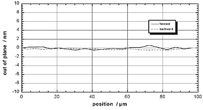
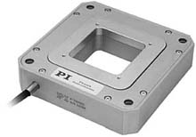
PI’s phenomenal experience in constructing nanomechanical parts was mobilized to meet this difficult challenge. We have developed over a hundred different nanopositioning systems down the past 20 years. Our performance-proven expertise and resources were pooled together to design and develop the device depicted in Fig. 12, i.e., the P-731K022 nanopositioning stage. By using capacitive sensors, the unit provides sub-nanometric resolved travel, stability through a 100 x 100 µm travel range and flatness in the nanometric region (Fig. 13).
This is a legacy product that may have limited availability or may have been replaced. Ask a PI engineer for an equivalent new model.