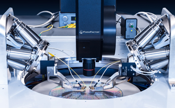
Automated, active optical alignment systems increase throughput in production of optics components and SIP photonics component packaging and testing, significantly. Running multiple tasks and algorithms fast and in parallel is key to big time savings. Automated optical assembly and alignment systems can now bring down the manufacturing cycles for SiP fiber optical photonics components to a few minutes. Unlike the moderate precision required to probe electrical wafers, probing of an optical wafer is much harder because the minute dimensions of the optical waveguides on silicon photonics wafers (~150 to 200 nanometers). Everything is even much more delicate than what’s known with single mode optical glass fibers, where average core diameters are in the range of 9 microns. Nanopositioning equipment is, therefore, essential to provide the accuracy and resolution required to align precisely over such minute distances.
Software, Image Processing, Gantry Robots, Nanometer Precision

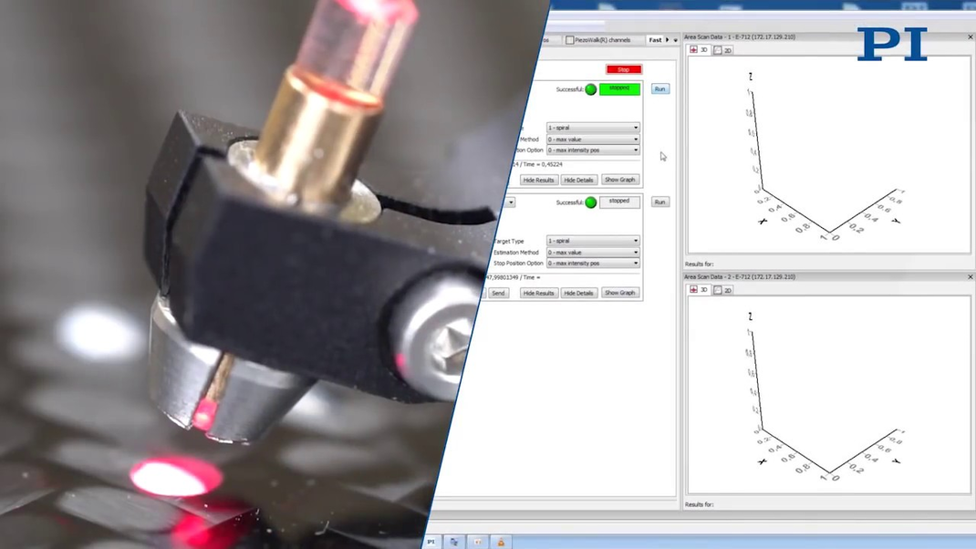
Nanopositioning mechanics alone is not enough to master the challenge of industrial scale automatic photonics packaging. New algorithms and advanced software need to work seamlessly together for success.
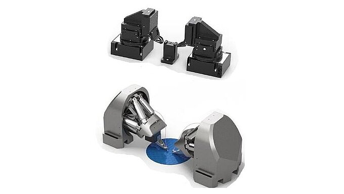
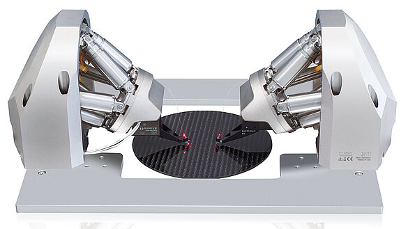
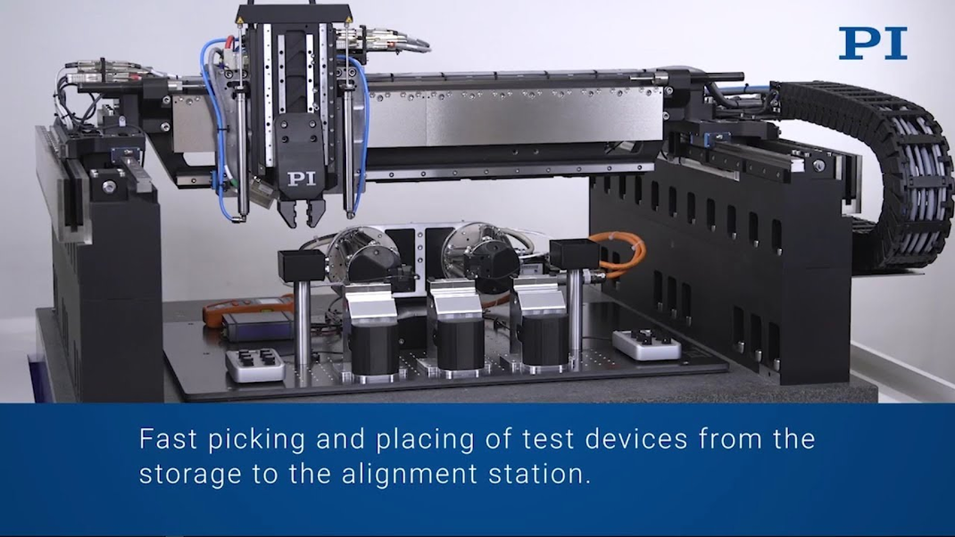
Adding vision guided robots for pick-and-place further improves throughput. Combinations of XYZ gantry robots and hexapod 6-axis robots with grippers have been suggested to enhance the scope.
Downloads
Alignment for Optics and Silicon Photonics
Fast Multi-Channel Photonic System
Silicon Photonics Set the Pace on the Data Highway
Automated Packaging As Complete Solution
Digital Brochure: Fast, Industrial, All-Digital Optical Alignment Subsystems
Unique capabilities address technical and economic requirements for test and packaging of silicon photonics and fiber optic devices