Ultra-High Precision AFM with 6-Axis Laser and Piezo Scanner for Traceable Measurements on Semiconductors and Step Standards
Atomic force microscopy (AFM) is used for surface measurements with resolution down to atomic levels – dimensions that are far beyond even the highest resolution optical microscopes. AFM is a noncontact procedure, with forces between a very fine measuring tip and the object surface revealing information about the topography, chemical surface condition, defects, etc. Atomic force microscopy is an established method used both in research and in production with applications including materials research, nano/bio-technology life sciences, and semiconductor inspection. High spatial resolution requires extreme precision for positioning both the measuring tip and the sample. Piezo-flexure scanned nanopositioning stages are well suited for this scanning method because they provide sub-nm resolution along with fast response and high scanning rates.
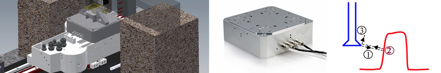
While atomic force microscopy is not a novelty, a “low noise metrological AFM” designed at the PTB (German Institute of Standards and Technology) is taking it to the next level (Figure 1). This system will be employed for traceable measurements of step standards (used to calibrate other AFMs) and CD critical dimension (smallest reproducible structures) measurements in the latest semiconductor generation.
Two Measurement Methods: Area Scan and Single Point Probing
Depending on the application, two measurement methods are available. In the Area Scan mode, the AFM tip is oscillated with constant frequency and amplitude and brought close to the sample at working distance. The sample is scanned under the tip. If the distance varies during scanning, a change can be seen in the frequency and amplitude of the tip and the Z-position of the sample is corrected in real-time until the oscillation stays constant. The topography information of the sample surface is then derived from the variation of the Z position together with the X and Y coordinates, which determine the spatial resolution.

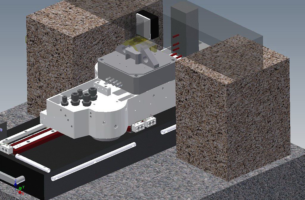
However, for surfaces edges with steep structures, the area scan method does not provide enough detail. The “Single Point Probing” mode solves this problem. Here, the positioning device slowly approaches a recognized step to measure it accurately (Figure 2). The direction of motion is the surface normal of the step, i.e. three active axes are required for sample positioning. The characteristic “curve of force”, a result of changing frequency, amplitude, and phase of the tip oscillation at different parts of the step, is captured. The measurement is repeated at different points, until the entire step is mapped. This measurement method is relatively slow, but returns very accurate information about topographically steep areas (high-aspect ratio). It is suitable, for example, also for quantitative measurements on semiconductor structures with very small dimensions from 10 to 20 nanometers.
High Demands on the Nanopositioning Scanner
The multi-axis sample scanner has to satisfy high precision and dynamics requirements in both measurement methods, in particular with regard to resolution. It must resolve down to the sub-nanometer range because the spatial resolution is directly related to the positioning system’s position resolution. At the same time, there are high requirements with regard to dynamics. A higher scanning speed in Z allows for a higher planar scanning speed. Higher speed means faster measurements and higher quality data at the same time, because the shorter measurements leave less time for position drift.
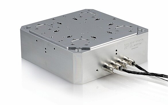
For the above reasons, PTB decided in favor of a parallel-kinematics piezo-flexure guided nanopositioning system (Figure 3). The closed-loop 6-axis system, designed and manufactured by market leader PI (Physik Instrumente), provides working ranges of 12 µm in three linear axes and positioning resolution better than 0.1 nanometers. Three rotary degrees of freedom are used for error compensation. Despite providing motion in all 6 degrees of freedom, the positioner has to be very compact to be fitted in the AFM.
Because the AFM is used for quantitative measurements, both position reproducibility and absolute accuracy are critical parameters. Piezo-flexure positioners – if designed well – provide frictionless, vibration-free and play-free motion – ideal conditions to precisely position and scan the sample in XY and Z. The additional three rotational axes are used for compensation of parasitic angular errors, resulting in unprecedented multi-axis accuracy. A high natural frequency above 1.4 kHz (@0.3kg load) further adds to the precision and stability, because external acoustic interferences do not affect the measurements.
Position Sensor Technology: Direct Metrology is Key
For the new atomic force microscope, PTB uses external differential interferometers to directly determine the motions between the AFM head and the sample in all six degrees of freedom. The interferometers provide very high dynamic bandwidth along with incredibly high resolution in the 10 picometer range and excellent linearity. This metrology method is even more direct than the stage-internal direct metrology system based on capacitive sensors. By measuring the position directly off the sample, disturbance effects such as drift or warping between the moving stage platform and the sample itself are eliminated and overall accuracy is further increased.
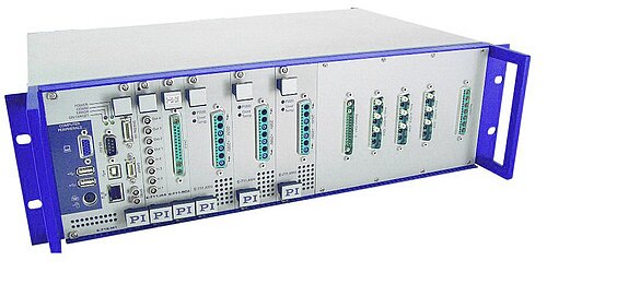
The interferometer signals are transmitted via a serial data stream to a multi-axis digital piezo controller (model PI, E-712). This controller can be precisely adapted to the positioning system and features complex error compensation math for all six-axes. The controller also provides finely tuned linearization algorithms for an extremely uniform run and fast feed motions with maximum force. By conjointly using parallel kinematics and interferometric measurement of all six degrees of freedom, the E-712 controller can correct unintended parasitic crosstalk (e.g. caused by external forces) in real time, applying corresponding algorithms.
Absolute-measuring, capacitive position sensors, integrated in the piezo stage, are used for the initialization before the measurement is started:
During initialization, the piezo stage relies on position information of the internal sensors to approach a defined starting position. For the measurement, the servo loop of the piezo stage is controlled by the external interferometers. While meeting PTB standards, they only measure motion rather than absolute positions.
The E-712 digital controller (Figure 4) can run in two closed-loop modes — internal (capacitive) and external (interferometric) capture of actual values, a prerequisite for the ultra-high precision surface topology measurement system developed by the PTB.
The advantages of piezo-based motion systems are convincing, and the drive that moves the measuring tip to the sample is also based on the piezo effect – a PiezoWalk® long travel linear motor. This motor design employs a combination of longitudinal and lateral piezo actuators to move the AFM tip over several millimeters with nanometer resolution to within working distance of the sample, before the measurement starts. After approaching the desired position, the self-clamping, high-force drive remains in an extremely stable position so as not to generate additional high-frequency oscillations between the AFM head and the six-axes positioning system.
AUTHOR: Gernot Hamann, Physicist, Business Development Manager for Microscopy at Physik Instrumente (PI) GmbH & Co. KG


Blog Categories
- Aero-Space
- Air Bearing Stages, Components, Systems
- Astronomy
- Automation, Nano-Automation
- Beamline Instrumentation
- Bio-Medical
- Hexapods
- Imaging & Microscopy
- Laser Machining, Processing
- Linear Actuators
- Linear Motor, Positioning System
- Metrology
- Microscopy
- Motorized Precision Positioners
- Multi-Axis Motion
- Nanopositioning
- Photonics
- Piezo Actuators, Motors
- Piezo Mechanics
- Piezo Transducers / Sensors
- Precision Machining
- Semicon
- Software Tools
- UHV Positioning Stage
- Voice Coil Linear Actuator
- X-Ray Spectroscopy