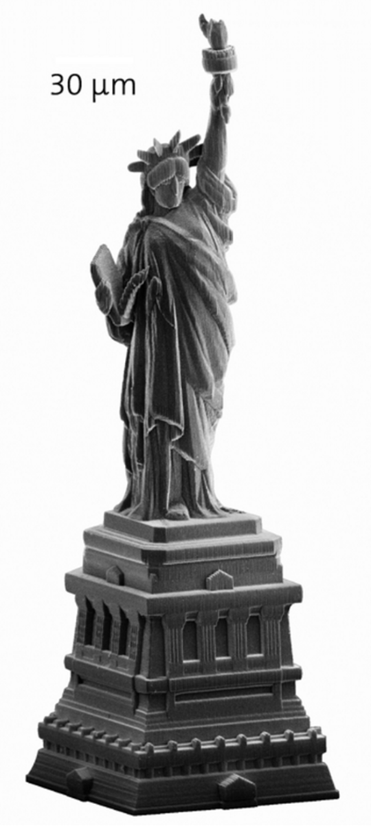
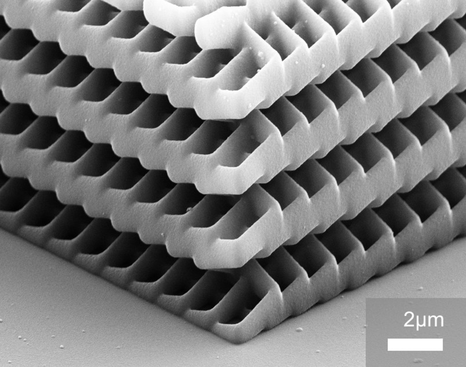
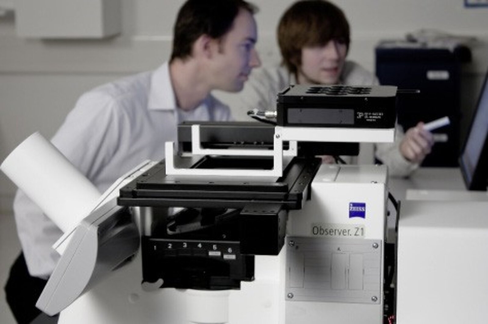
3D printing and additive manufacturing are gaining traction in prototyping and industrial manufacturing of complex parts. Typical 3D printers can produce feature sizes down to a few 10 microns. Significantly higher resolution is available with two photon polymerization and a new laser lithography system. Here the production of complex three-dimensional micro- and nanostructures is based on photosensitive materials. In addition to advanced laser technology, a motion system capable of controlling the focus and 3D position of the sample with nanometer precision within milliseconds is crucial. Piezo-flexure mechanisms, together with powerful digital motion controllers, take care of this aspect.
Track Widths Down to 150 Nanometers
The operating principle of the lithography process, which is compatible with commercially available photoresists, is easily understood: similar to a pen, moved in three dimensions, the laser beam can write arbitrary paths into the material with track widths from several micrometers down to 150 nanometers. Two-dimensional or 2.5 D structures are also feasible.
Highly focused ultra-short laser pulses cause a nonlinear optical process in the focal point. This lithography system can be used to fully automatically manufacture reproducible structures on sub-micron scales with design flexibility previously unknown.
High precision 3D lithography results rely on the capabilities of the corresponding nano-positioning and motion control system. “During the writing process, both the laser and the focus remain fixed, the sample is moved in three-dimensions,” explains Martin Hermatschweiler, CEO of Nanoscribe GmbH. “It is not sufficient to reach specific positions very accurately. The path here is just as important as the destination, which means the motion control system must also provide highly precise trajectory control. During the journey, we can then vary the laser intensity according to the acceleration or delay of the drive system in order to achieve the required lithography result.”

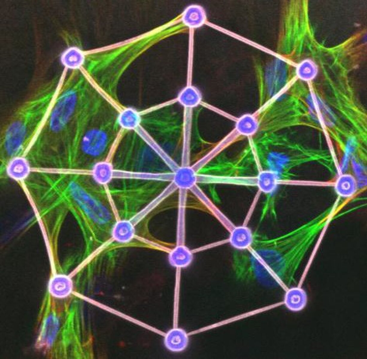
Typical fields of application for the new technology include the production of 3D matrices for cellular biology, the manufacture of micro-optical components or photonic crystals as well as rapid-prototyping and small production runs for microfluidic and nanofluidic systems.
The desired structures can be designed and imported using DXF format compatible CAD program, or alternatively using GWL script language specially designed to meet the needs of 3D structuring.
Frictionless Piezo Flexure Guided 3D Nanopositioning Drive
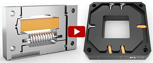
The demand for highly precise trajectory control is met by a parallel-kinematics piezo flexure nanopositioner with direct parallel position metrology and an advanced digital motion controller, both designed by PI.
More information on parallel-kinematic piezo designs.
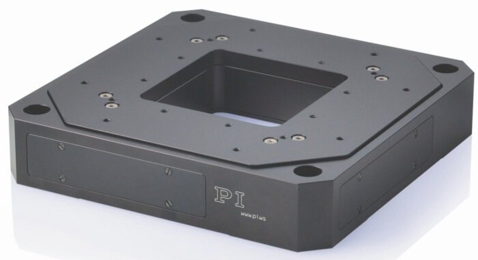
Nano-Scale Automation: P-563.3CD PImars XYZ piezo nanopositioning stage provides 300×300×300µm scanning range, sub-nanometer resolution with high-speed and trajectory precision due to its flexure-guided parallel kinematics piezo drive system and capacitive parallel metrology position feedback. A digital piezo motion controller delivers the computing performance and bandwidth required for highly accurate trajectory control along with powerful user software and drivers. Another direct laser writing lithography application of the piezo stage can be found here: “Fabrication of silver nano-rings using photo-reduction induced by femtosecond pulses”
Research at the University of Colorado on Two-Photon Photopolymerization for the Fabrication of Complex-Shaped Particles and Structures was conducted with a compact XYZ piezo nanopositioning stage, model P-611.3SF, featuring 100x100x100µm travel and 0.2nm resolution.


Blog Categories
- Aero-Space
- Air Bearing Stages, Components, Systems
- Astronomy
- Automation, Nano-Automation
- Beamline Instrumentation
- Bio-Medical
- Hexapods
- Imaging & Microscopy
- Laser Machining, Processing
- Linear Actuators
- Linear Motor, Positioning System
- Metrology
- Microscopy
- Motorized Precision Positioners
- Multi-Axis Motion
- Nanopositioning
- Photonics
- Piezo Actuators, Motors
- Piezo Mechanics
- Piezo Transducers / Sensors
- Precision Machining
- Semicon
- Software Tools
- UHV Positioning Stage
- Voice Coil Linear Actuator
- X-Ray Spectroscopy